Liquid crystal display device

a liquid crystal display and display device technology, applied in optics, instruments, transistors, etc., can solve the problems of large reduction of yield factor, lowering transmittivity, and applying a sufficient voltage, so as to reduce the yield factor and transmittivity.

Inactive Publication Date: 2005-02-24
PANASONIC LIQUID CRYSTAL DISPLAY CO LTD +1
View PDF14 Cites 32 Cited by
  • Summary
  • Abstract
  • Description
  • Claims
  • Application Information

AI Technical Summary

Benefits of technology

[0007] However, in Japanese Laid-open Patent Publication 111957 / 2000, pixel electrodes which apply an electric field to a liquid crystal layer are arranged on an upper portion of a color filter layer via through holes formed in the color filter layer. The through hole is formed for each pixel. However, inventors of the present invention have found a serious problem with respect to the mass-productiveness or the yield factor that the clogging of these through holes gives rise to the large reduction of the yield factor according to a result of an experiment. Further, in the IPS display type, the dielectric constant is low and due to the voltage dividing effect brought about by the color filter layer whose thickness is greater than a film thickness of an inorganic insulation film on the TFT. Accordingly, when the through holes are not formed as described in Japanese Laid-open Patent Publication 111957 / 2000, it is impossible to apply a sufficient voltage to the liquid crystal layer so that there arises a problem that the transmittivity is lowered.

Problems solved by technology

However, inventors of the present invention have found a serious problem with respect to the mass-productiveness or the yield factor that the clogging of these through holes gives rise to the large reduction of the yield factor according to a result of an experiment.
Accordingly, when the through holes are not formed as described in Japanese Laid-open Patent Publication 111957 / 2000, it is impossible to apply a sufficient voltage to the liquid crystal layer so that there arises a problem that the transmittivity is lowered.
However, color filters are not formed on the first substrate and there is no technical disclosure including problems related with the color-filter-on TFTs.
In this manner, there has been a problem that the steps are extremely long.
Further, such lengthy steps increases chances of positioning of exposure on the first substrate on which the TFTs are formed.
Accordingly, when the manufacturing steps are performed while ensuring the margin for positioning, there arises a problem that the original purpose of the color-filter-on TFTs to provide a bright liquid crystal display device by increasing the numerical aperture and the transmittivity is not achieved.

Method used


Image

  • Liquid crystal display device
  • Liquid crystal display device
  • Liquid crystal display device

Examples


embodiment 1

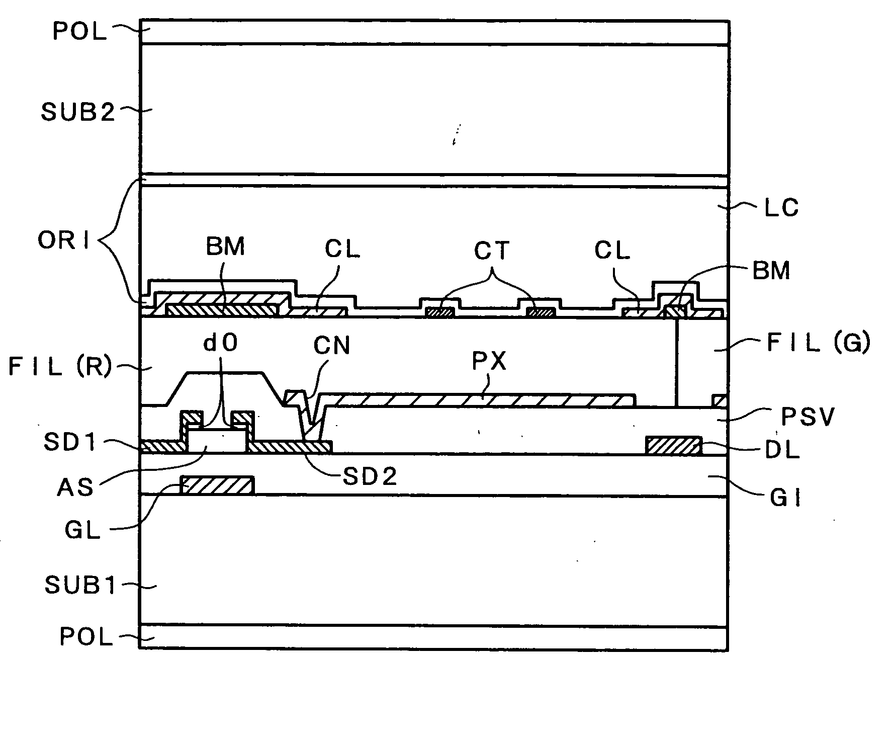
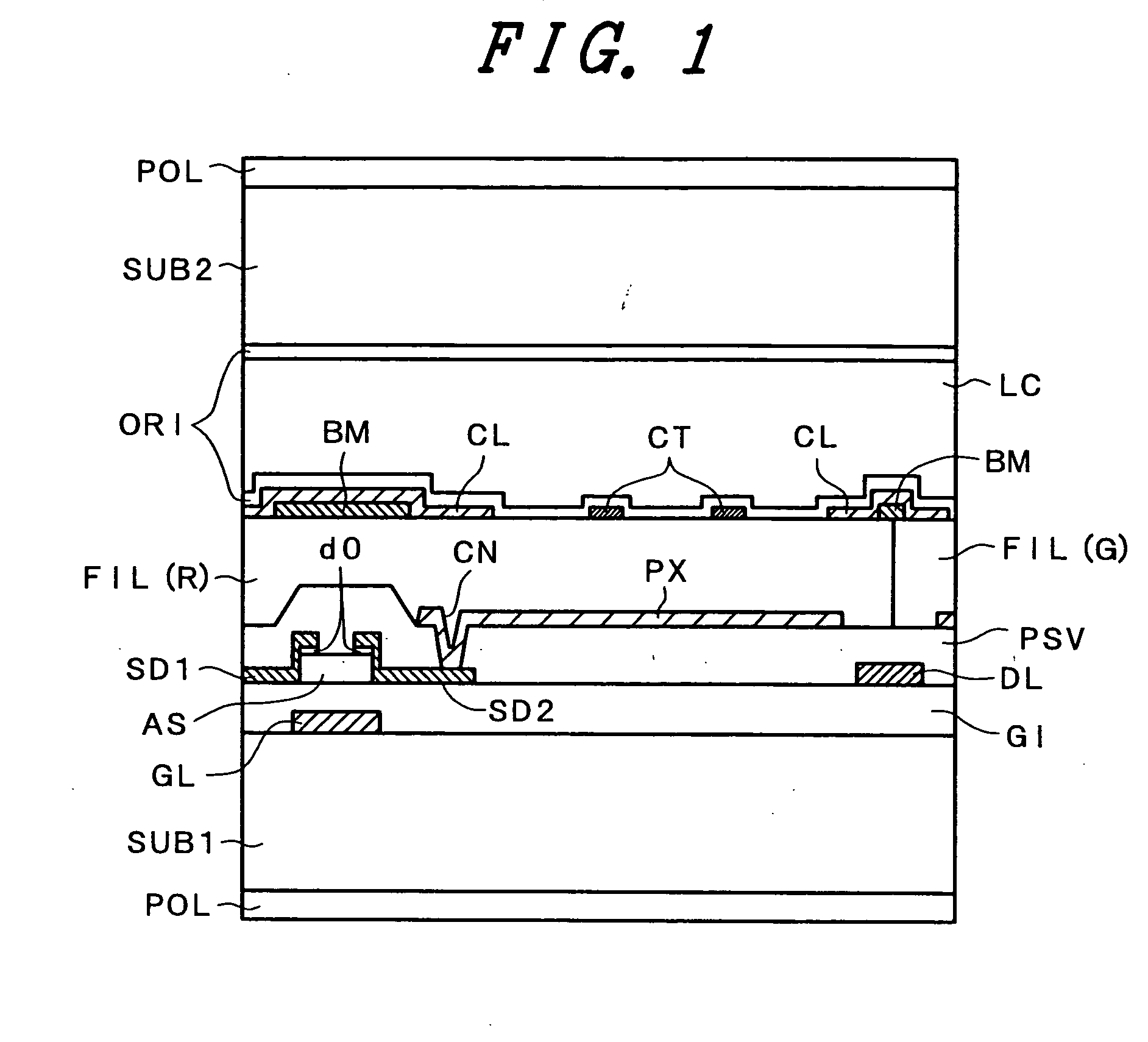
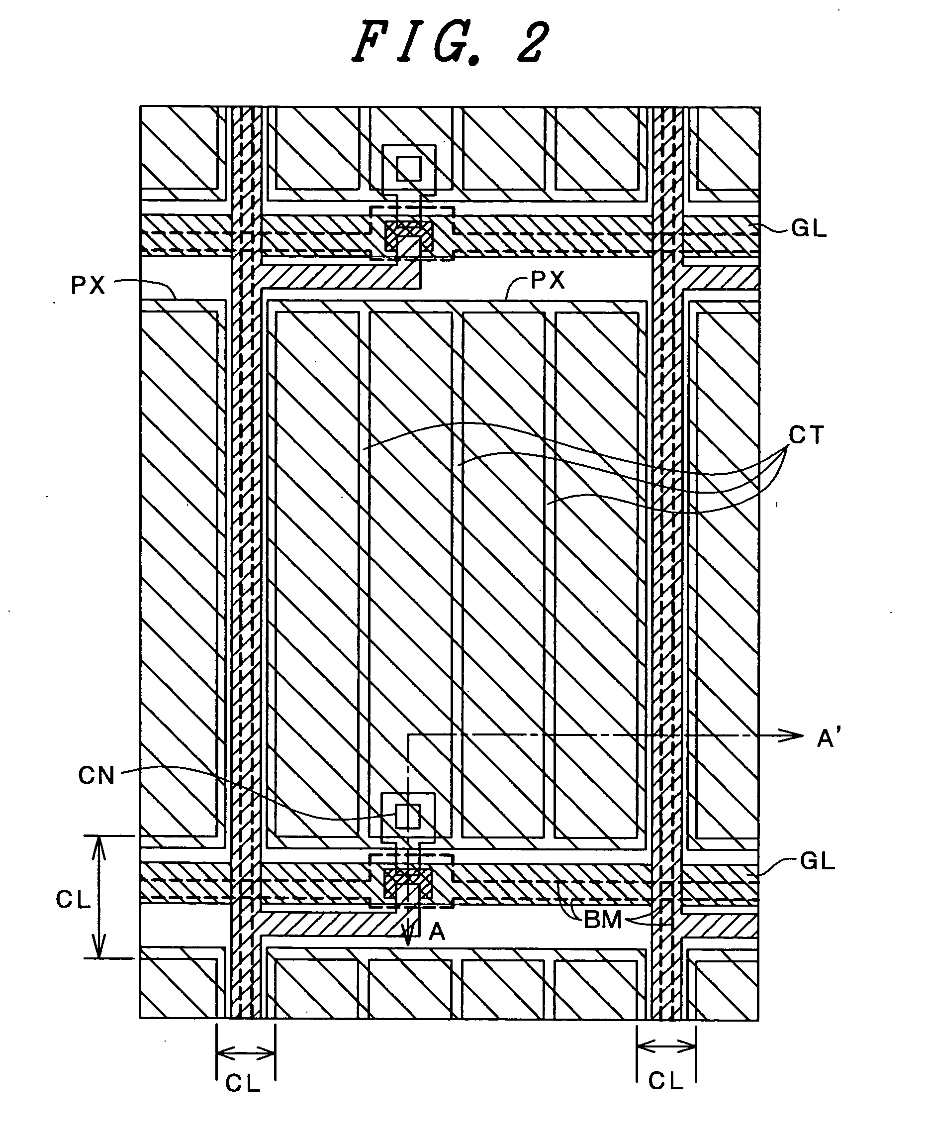
[0053]FIG. 1 and FIG. 2 show a structure of a pixel portion of a liquid crystal display device of a type according to the embodiment 1. FIG. 1 is a cross section taken along a line A-A′ of FIG. 2.

[0054] First of all, the embodiment is explained in conjunction with FIG. 1. Gate lines (gate electrodes) GL made of Mo, Cr or Al are arranged on a first substrate SUB1 which uses a glass substrate and a gate insulation film GI made of SiN is formed such that the gate insulation film GI covers the gate lines GL. A scanning driving voltage is supplied to the gate lines GL. Further, A semiconductor film AS which is made of amorphous silicon is arranged on the gate lines GL by way of the gate insulation film GI and functions as a channel layer of a thin film transistor (TFT). Further, drain electrodes SD1 and the source electrodes SD2 made of Mo, Cr or Al are arranged on the semiconductor layer film AS by way of semiconductor layers d0 doped with phosphorus at high concentration. A protective...

embodiment 2

[0080] The structural difference between this embodiment and the previous embodiment 1 is explained in conjunction with FIG. 6 and FIG. 7. Here, FIG. 6 shows a cross section taken along a line B-B′ in FIG. 7.

[0081] In a liquid crystal display device of this embodiment, gate lines GL and common electrode lines CL are arranged on a first glass substrate SUB1 and, further, common electrodes CT which are formed of transparent conductive films made of ITO or the like are arranged to be superposed on and are connected with the common electrode lines CL as shown in FIG. 7. These common electrodes CT take a rectangular shape in a plan view such that the common electrodes CT are not superposed on the gate lines GL and drain lines DL. The first glass substrate SUB1 is covered with a gate insulation film GI such that the gate insulation film GI covers the electrodes and the lines. Semiconductor layers AS, drain electrodes SD1 and source electrodes SD2 are formed on the gate insulation film GI...

embodiment 3

[0087]FIG. 8 shows a cross section of a liquid crystal display device of this embodiment. On a first glass substrate SUB1, gate lines GL which drive a scanning voltage, drain lines DL which supply a video signal voltage, drain electrodes SD1 which constitute portions of the drain lines DL, source electrodes SD2, a gate insulation film GI which is made of SiN, a protective film PSV, and pixel electrodes PX which are arranged on the protective film PSV and are connected with the source electrodes SD2 are formed. The structure and the manufacturing steps up to the pixel electrodes PX of this embodiment are as same as those of the embodiment 1.

[0088] The difference between this embodiment and the embodiment 1 lies in the structure disposed above the pixel electrodes PX within the pixels and the manufacturing steps corresponding to the structure. The color filter layers FIL are arranged such that, at the semiconductor layer AS of the TFT, on the color filter layer FIL(R) of a single col...


PUM

PropertyMeasurementUnit
thicknessaaaaaaaaaa
distanceaaaaaaaaaa
resistivityaaaaaaaaaa

Abstract

In a TFT type liquid crystal display device comprising first and second transparent substrates and a liquid crystal layer which is sandwiched between the first and second substrates, the first substrate includes a plurality of video signal lines, a plurality of scanning signal lines and a plurality of pixel regions which are formed as regions surrounded by the video signal lines and the scanning signal lines, each pixel region includes at least one active element, one pixel electrode and one common electrode, and color filter layers are formed between the pixel electrodes and the liquid crystal layer. The liquid crystal display device is substantially characterized in that the common electrodes are formed as layers above the color filters, the pixel electrodes are formed as layers below the color filters, and the color filters are superposed at least on the whole surfaces of the pixel electrodes in the pixel region.

Description

BACKGROUND OF THE INVENTION [0001] 1. Field of the Invention [0002] The present invention relates to a liquid crystal display device and a manufacturing method thereof. [0003] 2. Description of the Related Art [0004] An example of a basic constitution of a liquid crystal display device which uses thin film transistors (also referred to as “TFTs” in this specification) as driving elements is constituted as follows. TFTs, scanning lines or signal lines are formed on a first transparent substrate, color filters are formed on a second transparent substrate, and liquid crystal is inserted into a gap between the first and second transparent substrates while arranging a TFT forming surface or a color filter forming surface at the inside of the respective substrates. The TFTs on the first substrate are arranged on respective pixel regions. Further, with respect to color filters on the second substrate, color regions consisting of red (R), green (G), blue (B) are arranged in a stripe shape a...

Claims


Application Information

Patent Timeline
Patent Type & Authority Applications(United States)
IPC IPC(8): G02F1/1335G02F1/1343G02F1/1362H01L29/786
CPCG02F1/134363G02F1/136209G02F2001/136222G02F2001/134372G02F1/136227G02F1/134372G02F1/136222G02F1/1335
Inventor ONO, KIKUOOCHIAI, TAKAHIROOKE, RYUTARONAKAYOSHI, YOSHIAKIKURAHASHI, NAGATOSHI
Owner PANASONIC LIQUID CRYSTAL DISPLAY CO LTD
Why Eureka
Try Eureka