Mems based multi-polar electrostatic chuck

a multi-polar electrostatic chuck and magnet technology, applied in electrostatic charges, emergency protective circuit arrangements, capacitors, etc., can solve the problems of costly power supply and consumption considerations, deleterious effects on the wafer, and reduce the cost of power supply and consumption, so as to improve process control, efficient clamp the substrate, and fast response time

Inactive Publication Date: 2005-02-24
AXCELIS TECHNOLOGIES
View PDF25 Cites 55 Cited by
  • Summary
  • Abstract
  • Description
  • Claims
  • Application Information

AI Technical Summary

Benefits of technology

[0011] The present invention is generally directed to a multi-polar electrostatic chuck and method for cooling a semiconductor substrate. The multi-polar electrostatic chuck, for example, comprises a clamping plate that is operable to efficiently clamp the substrate thereto, and to cool or heat the substrate in a generally uniform manner thereacross, thereby improving process control. According to one example, the clamping plate comprises a semiconductor platform, wherein a first electrically conductive layer is formed over a top surface thereof. The first electrically conductive layer further comprises a plurality of portions that are electrically isolated from one another, therein defining a plurality of poles or electrodes of the electrostatic chuck. In another example, the clamping plate further comprises a plurality of electrically insulative protrusions formed over the first electrically conductive layer. The plurality of protrusions generally define a plurality of valleys therebetween, and extend a first distance from a top surface of the clamping plate, therein defining a gap between the substrate and the top surface.
[0012] In a first embodiment, the electrostatic chuck is operable to exhibit backside pressure control of a cooling gas within the gap between the substrate and a top surface of the clamping plate. The gap between the substrate or wafer and the top surface is made quite small (e.g., less than about 1 micron), wherein a volume of the gas within the gap is small. The small gas volume provides for a fast response time (e.g., on the order of about 10 mS), thereby permitting a cooling of the wafer to be activated or deactivated expeditiously. For example, by changing the gas pressure within the gap from about 1 Torr to about 100 Torr, a heat transfer coefficient (HTC) can be controlled from a value less than about 2 mW / cm2C to a value greater than about 400 mW / cm2C. In addition, by establishing a small gap, gas conduction is substantially in the free molecular regime, wherein thermal conduction is independent of the gap and depends primarily on cooling gas pressure, which can be made substantially uniform across the wafer. Accordingly, in the first embodiment, the present invention advantageously provides a very fast turn-on of backside, free molecular regime gas conduction to a hot or cold chuck surface, wherein heating or cooling of the wafer is dictated primarily by the cooling gas pressure.

Problems solved by technology

Such high temperatures (e.g., temperatures exceeding 400C), however, can have deleterious effects on the wafer.
Significantly high voltages, however, can have deleterious effects on the wafer (e.g., a cause of particle generation), and may further have costly power supply and consumption considerations, along with increased failure rates.
However, conventionally machining an insulating layer 40 comprised of a ceramic typically has several drawbacks, both in terms of precision, as well as potential particulate concerns caused by the ceramic layer during wafer processing.
Furthermore, it is typically very difficult to obtain a chuck surface flatness (i.e., control a waviness of the surface) of less than 5 microns across a 300 mm workpiece using conventional mechanical machining methods.
This gap, however, is not uniform across wafer, and further varies depending on clamping conditions.
This relatively large and uncontrollable gap width across the wafer typically results in a lower cooling capability and a non-uniform temperature across the wafer.
Still further, electrical connections to electrodes of the ESCs of the prior art have typically proven to be difficult to form.
Such soldering can disadvantageously perturb the heat conduction uniformity across the wafer.

Method used


Image

  • Mems based multi-polar electrostatic chuck
  • Mems based multi-polar electrostatic chuck
  • Mems based multi-polar electrostatic chuck

Examples


Embodiment Construction

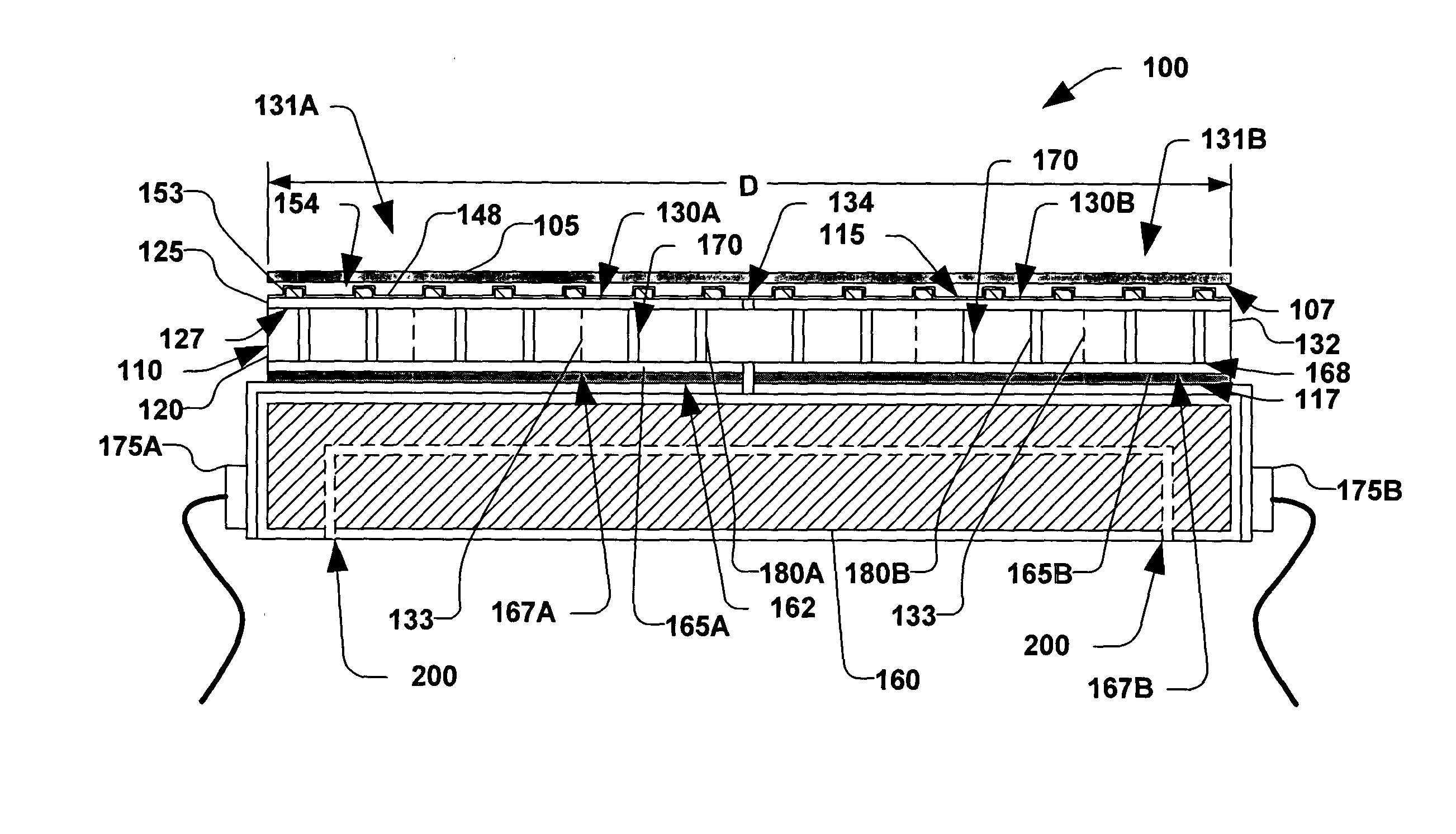
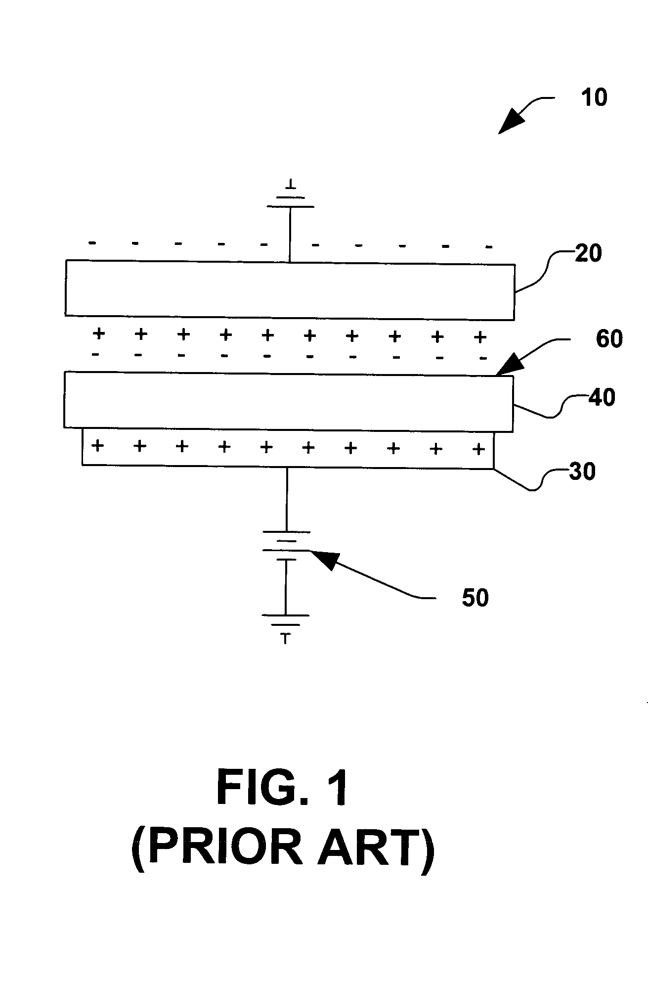
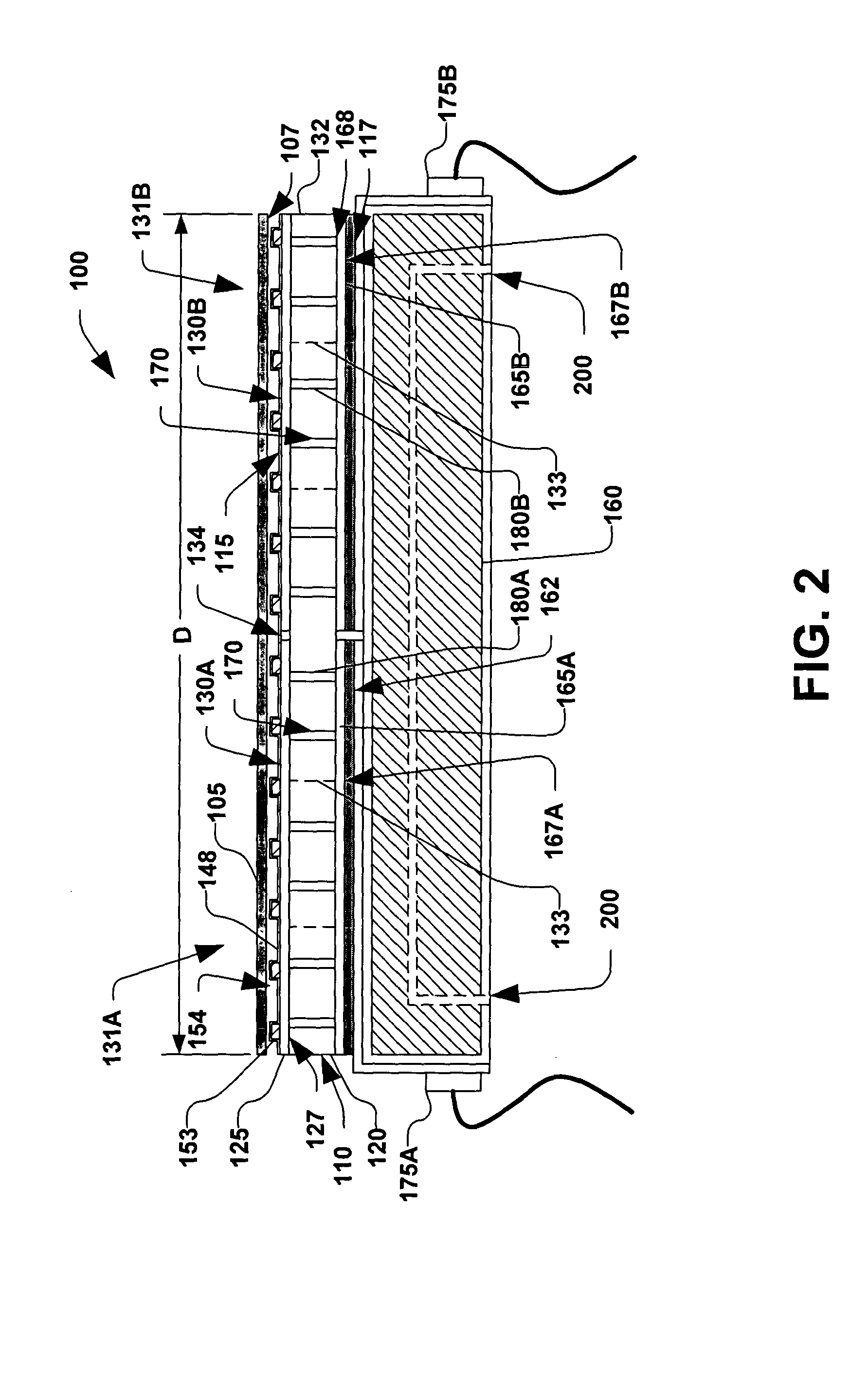
[0038] The present invention is directed towards a multi-polar electrostatic chuck (ESC) and an associated system and method that incorporates several inventive features thereof. In particular, the electrostatic chuck of the present invention increases an ability to rapidly and uniformly cool or heat a wafer substrate, for example, during an ion implantation process. Accordingly, the present invention will now be described with reference to the drawings, wherein like reference numerals are used to refer to like elements throughout. It should be understood that the description of these aspects are merely illustrative and that they should not be taken in a limiting sense. In the following description, for purposes of explanation, numerous specific details are set forth in order to provide a thorough understanding of the present invention. It will be evident to one skilled in the art, however, that the present invention may be practiced without these specific details.

[0039] The presen...


PUM


Abstract

The present invention is directed to a semiconductor processing apparatus and a method for clamping a semiconductor substrate and controlling a heat transfer associated therewith. According to one aspect of the present invention, a multi-polar electrostatic chuck and associated method is disclosed which provides a controlled and uniform heat transfer coefficient across a surface thereof. The multi-polar electrostatic chuck comprises a semiconductor platform having a plurality of protrusions that define gaps therebetween, wherein a distance or depth of the gaps is uniform and associated with a mean free path of the cooling gas therein. The electrostatic chuck is permits a control of a backside pressure of a cooling gas within the plurality of gaps to thus control a heat transfer coefficient of the cooling gas. The plurality of protrusions further provide a uniform contact surface, wherein a contact conductivity between the plurality of protrusions and the substrate is controllable and significantly uniform across the substrate.

Description

FIELD OF THE INVENTION [0001] The present invention relates generally to semiconductor processing systems, and more specifically to an apparatus and method for clamping a substrate and transferring thermal energy associated therewith. BACKGROUND OF THE INVENTION [0002] Processing of silicon wafers is commonplace in the manufacture of modern microelectronics devices. Such processing, including plasma processing and ion implantation may be performed at low pressures, wherein RF or microwave plasmas are delivered to the wafer, therein producing high temperatures at the wafer during processing. Such high temperatures (e.g., temperatures exceeding 400C), however, can have deleterious effects on the wafer. [0003] For many processes, precise temperature control is not required, as long as the wafer temperature remains at less than a predetermined limit, such as 400C or below. Current trends in ion implantation, however, are tending toward high power serial implanters which generally requir...

Claims


Application Information

Patent Timeline
Patent Type & Authority Applications(United States)
IPC IPC(8): H01L21/683
CPCH01L21/6875H01L21/6833H01L21/02
Inventor KELLERMAN, PETER L.OIN, SHUBROWN, DOUGLAS A.
Owner AXCELIS TECHNOLOGIES
Why Eureka
Try Eureka