Device transfer method and panel

a technology of device and transfer method, applied in the direction of basic electric elements, electrical apparatus, semiconductor devices, etc., can solve the problems of above-described cutting method, and difficulty in detecting the device itself, so as to prevent the resin layer covering the device, improve the strength of the resin buried device, and the panel is convenient to use.

Inactive Publication Date: 2005-02-24
SONY CORP
View PDF4 Cites 9 Cited by
  • Summary
  • Abstract
  • Description
  • Claims
  • Application Information

AI Technical Summary

Benefits of technology

[0016] With this configuration, it is possible to provide an inexpensive panel.
[0017] In the above device transfer method, preferably, connection holes are formed in the resin layer in a manner such as to reach the devices by laser beams, and the electrodes are connected to the devices via the connection holes. With this configuration it is possible to prevent the resin layer covering the device from being thinned and hence to improve the strength of the resin buried device.
[0018] In the device transfer method, preferably, the electrodes are each formed with their planar dimension substantially corresponding to a planar dimension of each of the resin buried devices, and the resin layer is cut by laser beams with the electrodes taken as a mask, to obtain the resin buried devices. With this configuration, it is possible to eliminate the need of use of a laser system having a high accurate positioning function and hence to reduce the production cost of the devices.

Problems solved by technology

The above-described cutting method, however, has problems.
As a result, if the sapphire substrate is full cut into chips by a dicer such as a diamond blade, problems such as cracking and / or chipping tend to occur in the cut planes of the sapphire substrate which prevent the sapphire substrate from being smoothly cut into chips of desired shapes and sizes, the dicer itself may also be broken, and that since sapphire has no cleavage characteristic, it is difficult to cut the sapphire substrate into chips by forming scribing lines on the sapphire substrate and forcibly cutting the sapphire substrate along the scribing lines by an external force.
However, such a cutting method, requires several steps including the labor intensive step of polishing the sapphire substrate 60.
In other words, the above method of cutting a sapphire substrate 60 is expensive and time consuming.
However, if the size of each LED device becomes as small as several tens of μm per side, it becomes difficult to handle the LED device in the transfer step.
Further, since an electrode of each device to be connected to a wiring layer of a base body of a display panel becomes small, the connection work becomes difficult and also a connection failure may often occur.

Method used


Image

  • Device transfer method and panel
  • Device transfer method and panel
  • Device transfer method and panel

Examples


Embodiment Construction

[0032] Hereinafter, embodiments of the present invention will be described in detail with reference to the accompanying drawings.

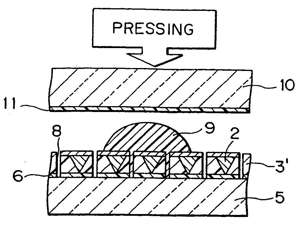
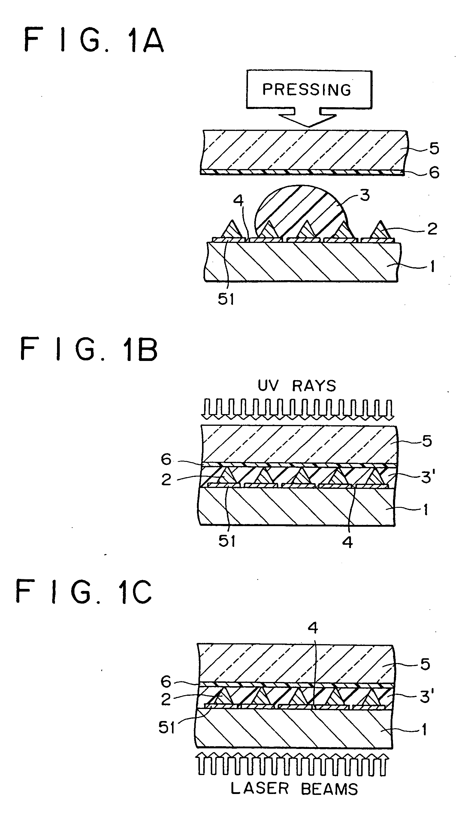
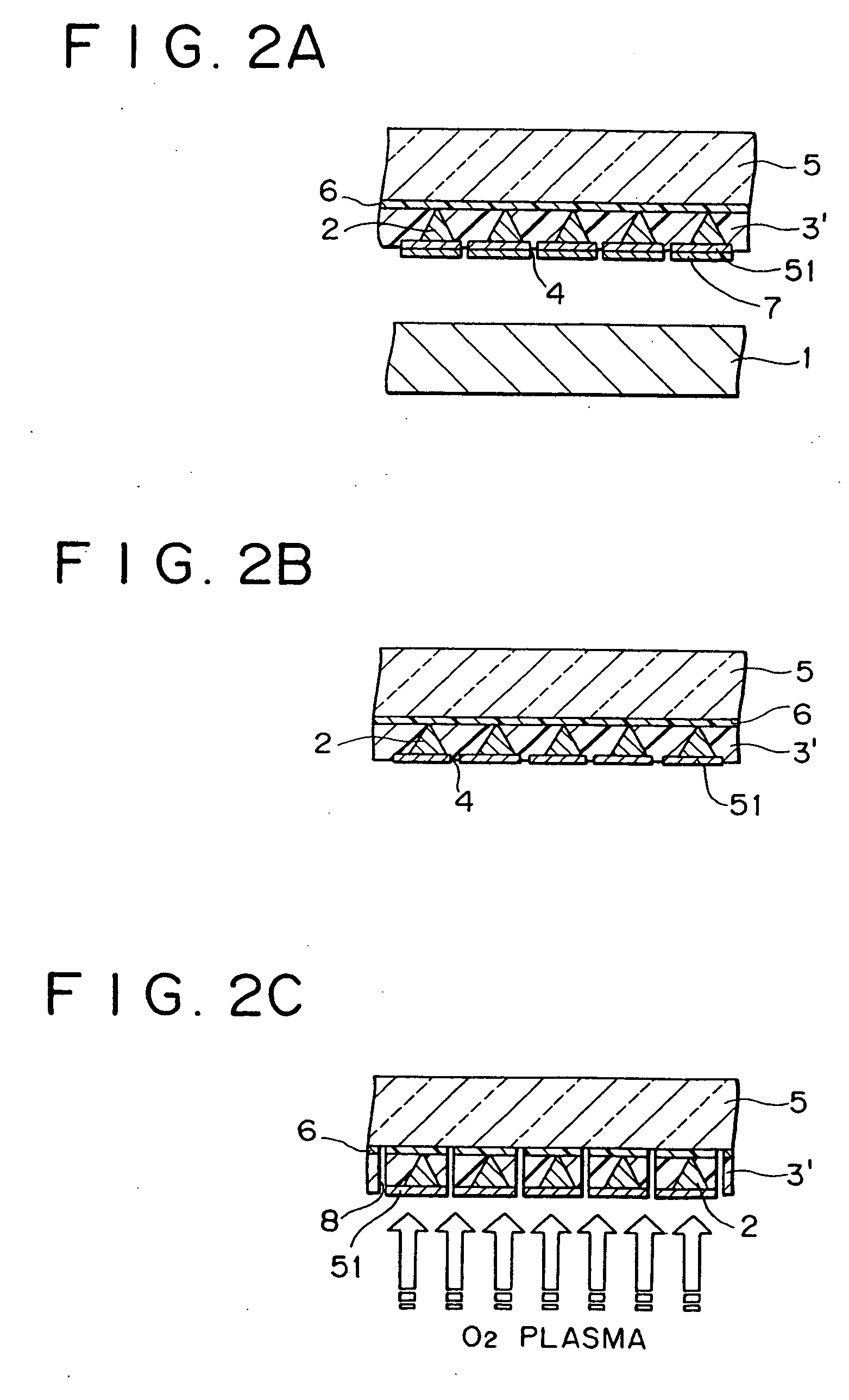
[0033] First, there will be described devices used for carrying out the present invention with reference to FIGS. 11A and 11B, which devices are exemplified by light emitting diodes representative of light emitting devices in the following embodiments. FIG. 11A is a sectional view of such a light emitting diode and FIG. 11B is a plan view of the light emitting diode. As shown in these figures, a light emitting diode 2 is made from a gallium nitride (GaN) based semiconductor and is formed by crystal growth on a device formation substrate, for example, a sapphire substrate 1.

[0034] An under growth layer 51 made from a GaN based semiconductor is formed on the sapphire substrate 1, and a hexagonal pyramid shaped GaN layer 52 doped with silicon is formed on the under growth layer 51 as follows: namely, an insulating film 53 is formed on the under growth layer...


PUM


Abstract

A device transfer method includes the steps of: covering a plurality of devices, which have been formed on a substrate, with a resin layer; forming electrodes in the resin layer in such a manner that the electrodes are connected to the devices; cutting the resin layer, to obtain resin buried devices each containing at least one of the devices; and peeling the resin buried devices from the substrate and transferring them to a device transfer body. This device transfer method is advantageous in easily, smoothly separating devices from each other, and facilitating handling of the devices in a transfer step and ensuring good electric connection between the devices and external wiring, even if the devices are fine devices.

Description

CROSS REFERENCE TO RELATED APPLICATIONS [0001] This patent application is a continuation of U.S. application Ser. No. 10 / 062,776, filed on Jan. 30, 2002, the disclosure of which is herein incorporated by reference.BACKGROUND OF THE INVENTION [0002] The present invention relates to a device transfer method of transferring light emitting devices such as light emitting diodes, which have been formed on a substrate, for example, a sapphire substrate, to a device transfer body such as a display panel, and to a panel on which the transferred devices are arrayed. [0003] A known method of producing an LED (Light Emitting Diode) display using LEDs includes the steps of cutting an LED wafer, which is obtained by stacking semiconductor layers on a device formation substrate, into chips by a diamond blade or the like, and transferring the LED chips to a display panel or the like with a pitch larger than an array pitch of the LED chips on the device formation substrate. [0004] The above-describe...

Claims


Application Information

Patent Timeline
Patent Type & Authority Applications(United States)
IPC IPC(8): H01L21/60H01L21/68H01L25/075H01L33/32H01L33/38H01L33/42H01L33/56
CPCH01L21/6835H01L2924/12041H01L24/82H01L25/0753H01L2221/68359H01L2221/68368H01L2224/24226H01L2924/01004H01L2924/01012H01L2924/01013H01L2924/01015H01L2924/01039H01L2924/01049H01L2924/01078H01L2924/01079H01L2924/01082H01L2924/10329H01L2924/01005H01L2924/01006H01L2924/01033H01L24/24H01L2224/24H01L2924/12042H01L2924/00H01L2924/00012
Inventor YANAGISAWA, YOSHIYUKIOOHATA, TOYOHARUIWAFUCHI, TOSHIAKI
Owner SONY CORP
Why Eureka
Try Eureka