Method for forming pattern and drop discharge apparatus

Inactive Publication Date: 2005-02-24
SEMICON ENERGY LAB CO LTD
View PDF37 Cites 97 Cited by
  • Summary
  • Abstract
  • Description
  • Claims
  • Application Information

AI Technical Summary

Benefits of technology

[0018] According to this invention, with the above-described structure, a pattern can be formed with improved position accuracy at the time of drop composition's landing on a substrate. Moreover, reduction in proce

Problems solved by technology

While the drop discharge method has many advantages, there are various limitations on drops containing compositions and substrates for actually performing fine patterning.
However, the actual drop landing accuracy is approximately some μm to 30 μm, and even afte

Method used


Image

  • Method for forming pattern and drop discharge apparatus
  • Method for forming pattern and drop discharge apparatus
  • Method for forming pattern and drop discharge apparatus

Examples


Example

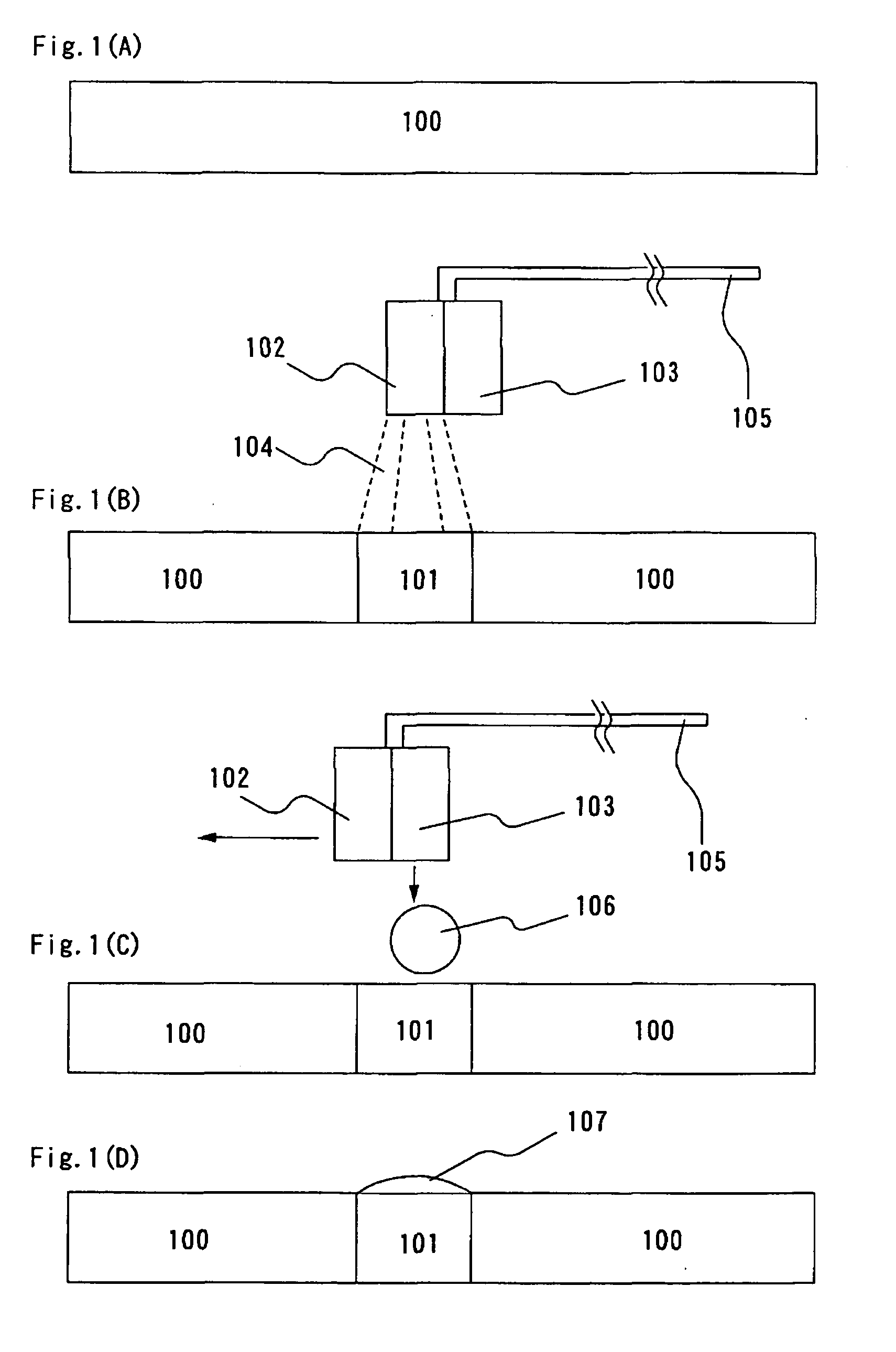
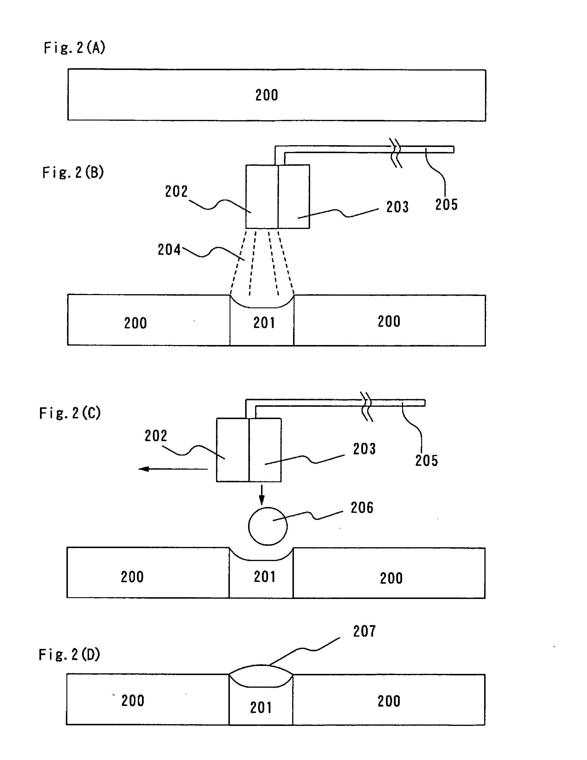
[0069] [Embodiment 1]

[0070] An embodiment of this invention will be described with reference to FIGS. 8 to 11.

[0071]FIG. 8(A) shows a step of forming a conductive coating for forming a gate electrode and a wiring.

[0072] An optically transparent substrate of glass, quartz or the like is used, but the substrate to be used is not limited to an optically transparent and any other substrate may be used as long as it is durable against the processing temperature at each step. As for the size of a substrate 1500, it is preferred to use a large-area substrate having a size of 600 mm by 720 mm, 680 mm by 880 mm, 1000 mm by 1200 mm, 1100 mm by 1250 mm, 1150 mm by 1300 mm, 1500 mm by 1800 mm, 1800 mm by 2000 mm, 2000 mm by 2100 mm, 2200 mm by 2600 mm, or 2600 mm by 3100 mm, so as to reduce the manufacturing cost. On the substrate 10, a conductive film 11 of aluminum, titanium, tantalum, molybdenum or the like is formed by film forming means having a nozzle unit in which plural discharge port...

Example

[0089] [Embodiment 2]

[0090] Using the display device formed by carrying out this invention, a television receiver, a computer and a video reproducing apparatus illustrated in FIG. 13 and other electronic devices can be completed.

[0091]FIG. 13(A) shows an example of completing a television receiver by applying this invention. The television receiver is constituted by a casing 2001, a supporting stand 2002, a display unit 2003, speaker units 2004, a video input terminal 2005 and the like. By utilizing this invention, particularly a television receiver with a screen size of 30 inches or more can be manufactured at a low cost. Moreover, by utilizing this invention, the television receiver can be completed.

[0092]FIG. 13(B) shows an example of completing a notebook model personal computer by applying this invention. The personal computer is constituted by a body 2201, a casing 2202, a display unit 2203, a keyboard 2204, an outer connection port 2205, a pointing mouse 2206 and the like. ...

Example

[0094] [Embodiment 3]

[0095] In this embodiment, a method of filling a contact hole (opening) with a drop composition by using the drop discharge method will be described with reference to FIGS. 14 to 16.

[0096] In FIG. 14(A), a semiconductor 3001 is provided on a substrate 3000, and an insulator 3002 is provided on the semiconductor 3001. The insulator 3002 has a contact hole 3003. As a method for forming the contact hole, a known method may be used, alternatively the drop discharge method may also be used. In this case, a wet etching solution is discharged from a nozzle, thereby forming the contact hole 3003. In this way, formation of a contact hole and formation of a wiring can be continuously carried out by the drop discharge method.

[0097] Then, a nozzle 3004 is moved to a position above the contact hole 3003 and continuously discharges a drop composition into the contact hole 3003 to fill the contact hole 3003 with the drop composition (FIG. 14(B)). After that, as the position ...


PUM


Abstract

The present invention is characterized in having a process for forming a pattern by making a substrate having an insulating property, such as a liquid-repellent thin film over a substrate, such as a semiconductor film, selectively have affinity for liquid by plasma generating means 102, and discharging a drop compound to the surface having affinity for liquid by a drop discharging means 103. By putting the region having affinity for liquid, which was selectively formed, between liquid-repellent, a drop after drop landing can be formed without moving the drop landing portion

Description

TECHNICAL FIELD [0001] This invention relates to a method for forming a film pattern and a drop discharge apparatus. BACKGROUND ART [0002] Recently, development of methods for forming patterns using a drop discharge method based on screen printing or ink jet has been actively carried out. [0003] Since the drop discharge method has many advantages including need for no masks because of its patterning by direct plotting, easy application of the method to a large substrate, high material use efficiency and the like, use of fine patterning for FPDs (flat panel displays) has become popular. [0004] As applications of the method, formation of not only light-emitting layers of organic EL (electroluminescence) and color filters of LCDs (liquid crystal displays) but also electrodes and organic transistors of PDPs (plasma display devices) has been reported. DISCLOSURE OF THE INVENTION [0005] (Problems to be Solved by the Invention) [0006] While the drop discharge method has many advantages, th...

Claims


Application Information

Patent Timeline
IPC IPC(8): B05B17/06H01L21/20H01L21/288H01L21/768H01L51/00H01L51/40
CPCB05B17/0607H01L21/288H01L51/0021H01L21/76877H01L51/0004H01L21/76838H10K71/13H10K71/60B05D1/26B05D3/04B05C5/00B05C9/10
Inventor MAEKAWA, SHINJIYAMAZAKI, SHUNPEI
Owner SEMICON ENERGY LAB CO LTD
Why Eureka
Try Eureka