

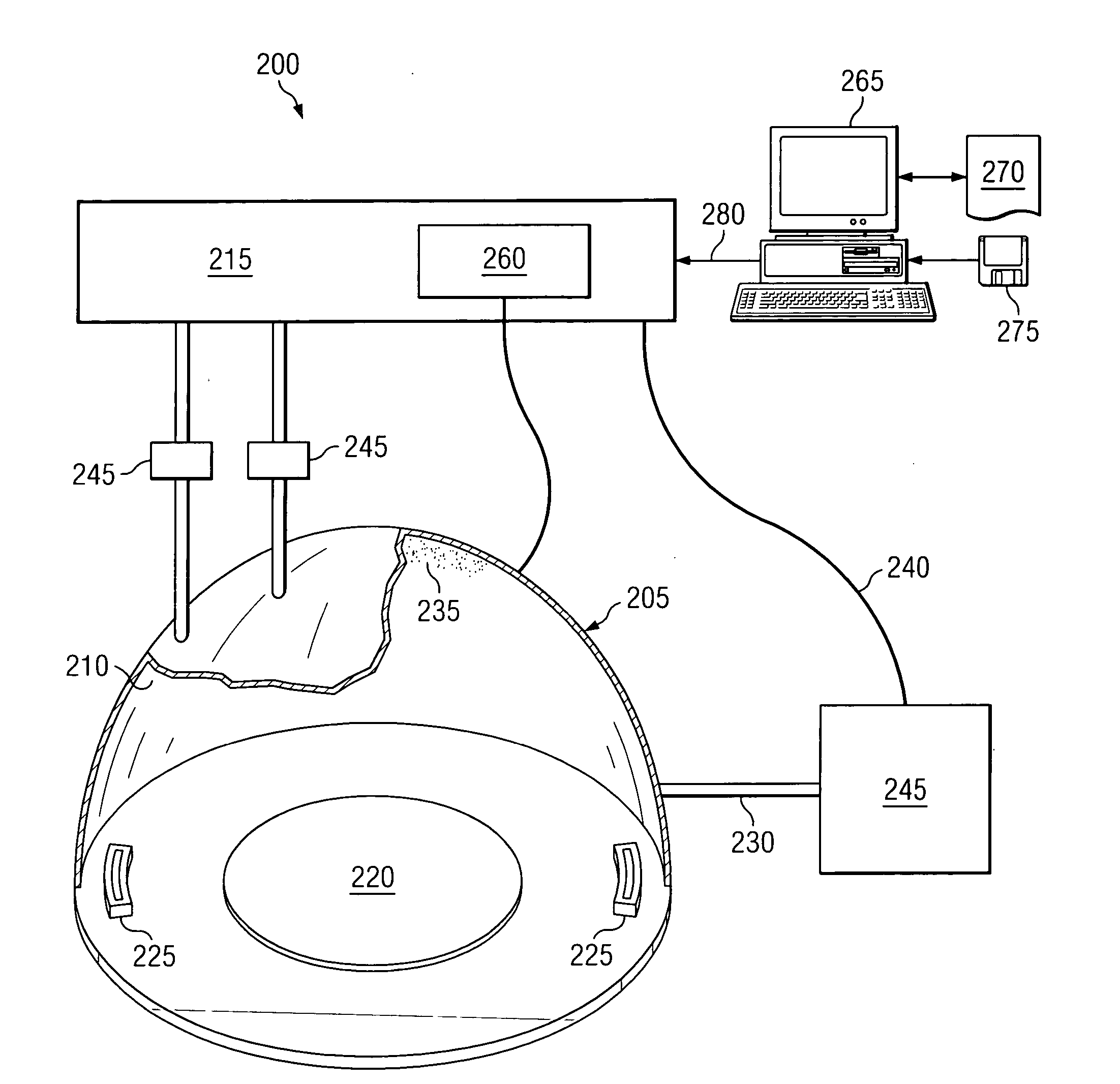
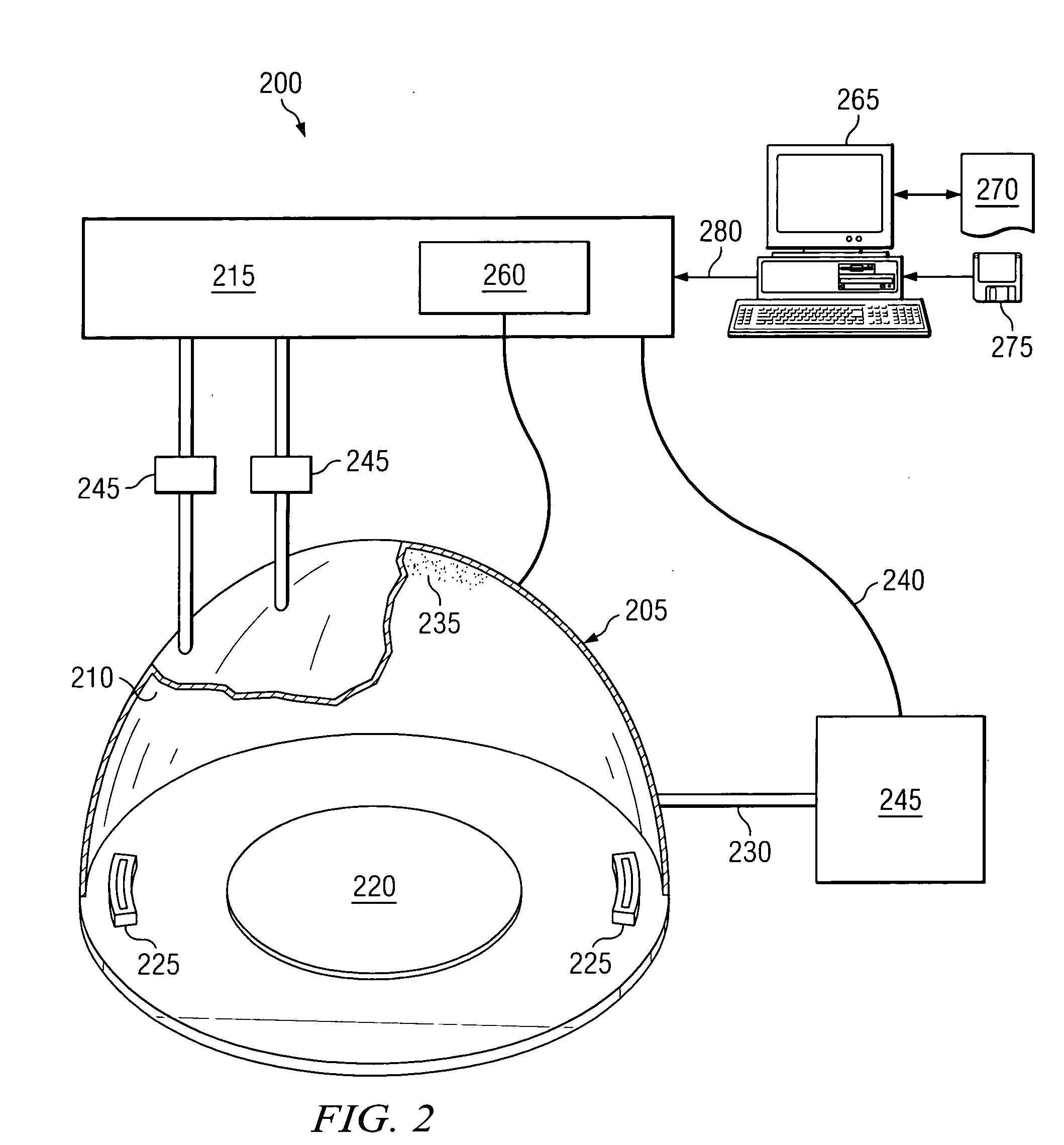
Deposition tool cleaning process having a moving plasma zone
a technology of deposition tool and cleaning process, which is applied in the direction of cleaning hollow objects, liquid cleaning, coatings, etc., can solve the problems of reducing the uniformity of the deposited layer on the substrate, the overall quality of the device, and the effect of preventing the accumulation of localized metal compound deposits
- Summary
- Abstract
- Description
- Claims
- Application Information
AI Technical Summary
Benefits of technology
Problems solved by technology
Method used
Image

Examples
examples
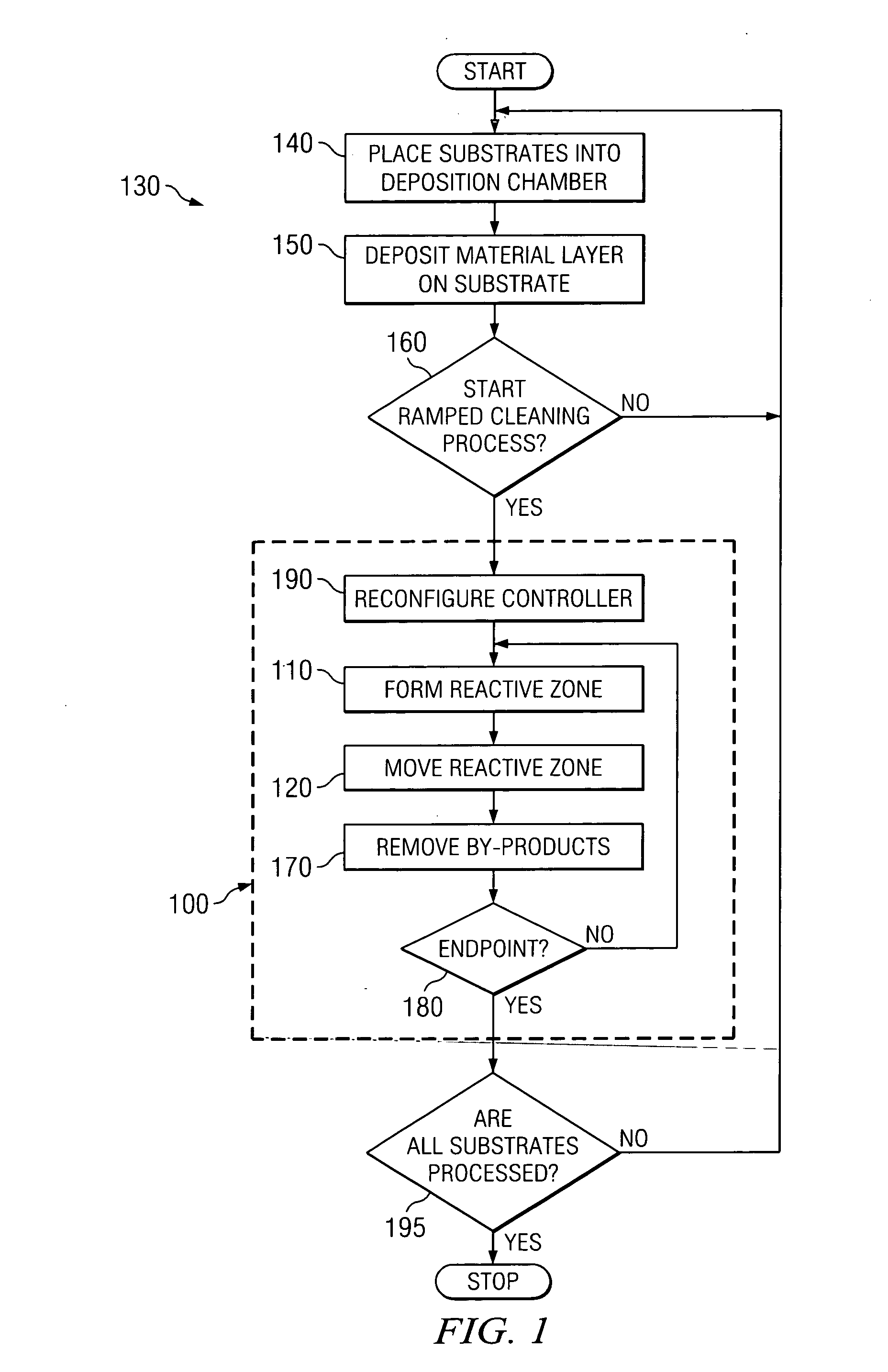
[0045] The following examples are presented to illustrate the effectiveness of the ramped cleaning process of the present invention as compared to a conventional two-step cleaning process. A single-chambered HDPCVD tool (Novellus Sequel System, San Jose, Calif.) having one substrate station was used. For test purposes, about 4500 Angstrom thick layers of FSG, comprising about 4.5 percent fluorine and balance silicon dioxide, were deposited on silicon wafers using a conventional HDPCVD process. The tool was configured to run an intermittent in situ cleaning processes between every 6 micron deposition of FSG.
[0046] For illustrative purposes, the results for two in situ cleaning processes are compared: a conventional two-step cleaning process and a ramped cleaning process of the present invention. For both cleaning processes, the pressure inside the chamber was maintained at about 2 Torr and the radio-frequency power used for plasma generation was about 4300 Watts. The flow rate of NF...
PUM
| Property | Measurement | Unit |
|---|---|---|
| pressure | aaaaa | aaaaa |
| power | aaaaa | aaaaa |
| power | aaaaa | aaaaa |
Abstract
Description
Claims
Application Information