Method to produce transistor having reduced gate height

a technology of integrated circuit transistors and gate heights, which is applied in the direction of transistors, electrical devices, semiconductor devices, etc., can solve the problems of increasing the risk of gate impurity contamination of the underlying gate oxide, and avoiding the problem of dopant encroachment and silicide bridging. , the effect of reducing the achievable size of the spacer

Inactive Publication Date: 2005-03-03
GLOBALFOUNDRIES INC
View PDF16 Cites 65 Cited by
  • Summary
  • Abstract
  • Description
  • Claims
  • Application Information

AI Technical Summary

Benefits of technology

[0012] The artificial increase in gate height achieved with the sacrificial layer at the top of the gate stack allows the formation of larger disposable spacers. The invention uses a two-step spacer formation process for spacer width modulation

Problems solved by technology

Challenges are encountered during conventional processing of high-performance complementary metal oxide semiconductor (CMOS) devices.
Therefore, as the gate height is decreased, the risk of gate impurity contaminating the underlying gate oxide increases.
However, reducing the overall thermal budget can lead to insufficient dopant activation in other electrodes and as a result, drive currents may be limited.
Alternatively, the self-aligned gate/source/drain and halo implant energy may be drastically reduced to mitigate the dopant penetration; however, the low energy implants for the source/drain and the halo cause high source/drain parasitic resistance and insufficient halo doping in the channel, degrading drive currents and short-channel rolloff characteristics.
In addition, the maximum sidewall spacer length achievable with a gate of reduced height—poses challenges.
With the shorter gate height, the maximum size of the spacer is reduced due to the reduced step height for the RIE (reactive ion e

Method used


Image

  • Method to produce transistor having reduced gate height
  • Method to produce transistor having reduced gate height
  • Method to produce transistor having reduced gate height

Examples


Embodiment Construction

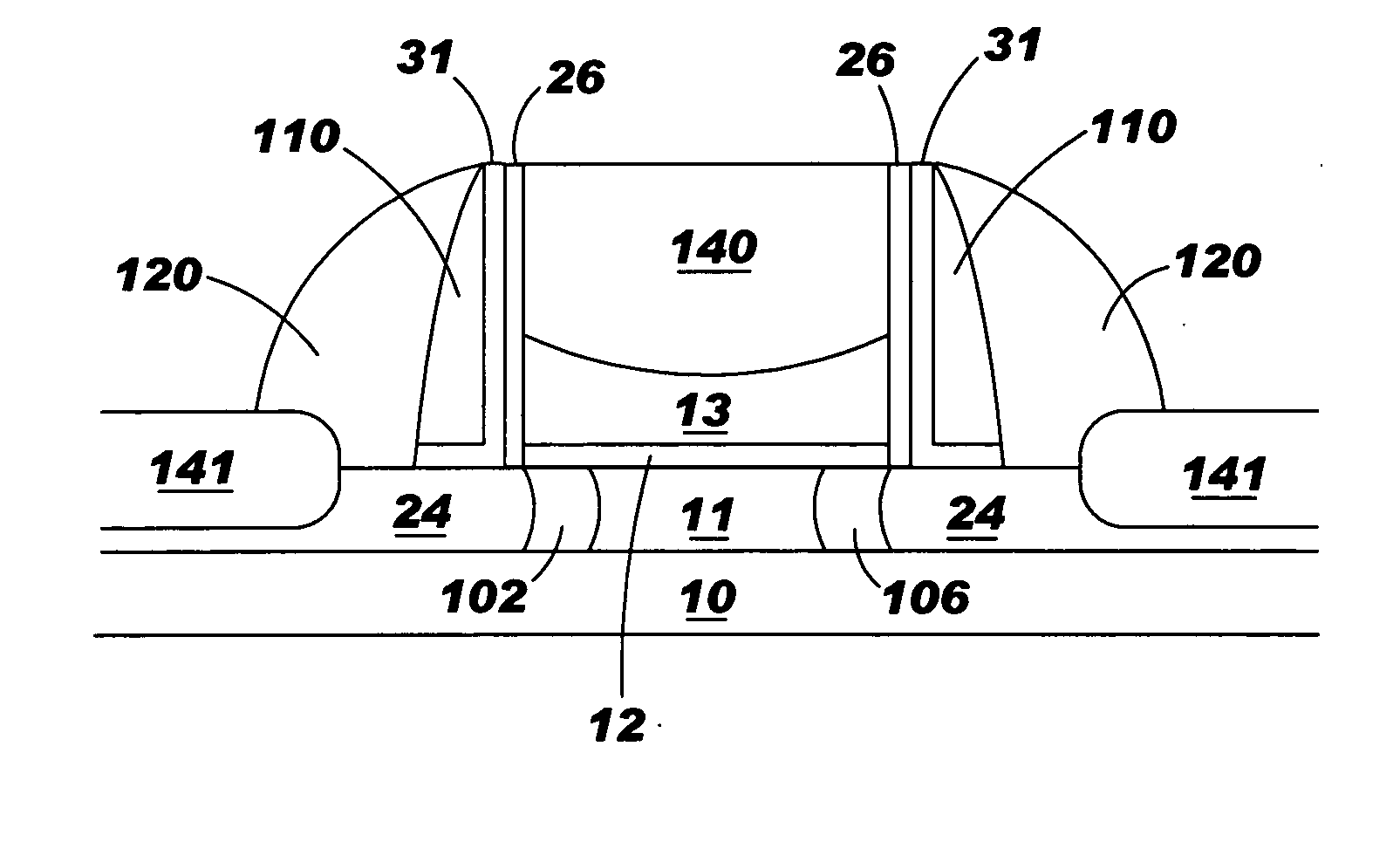
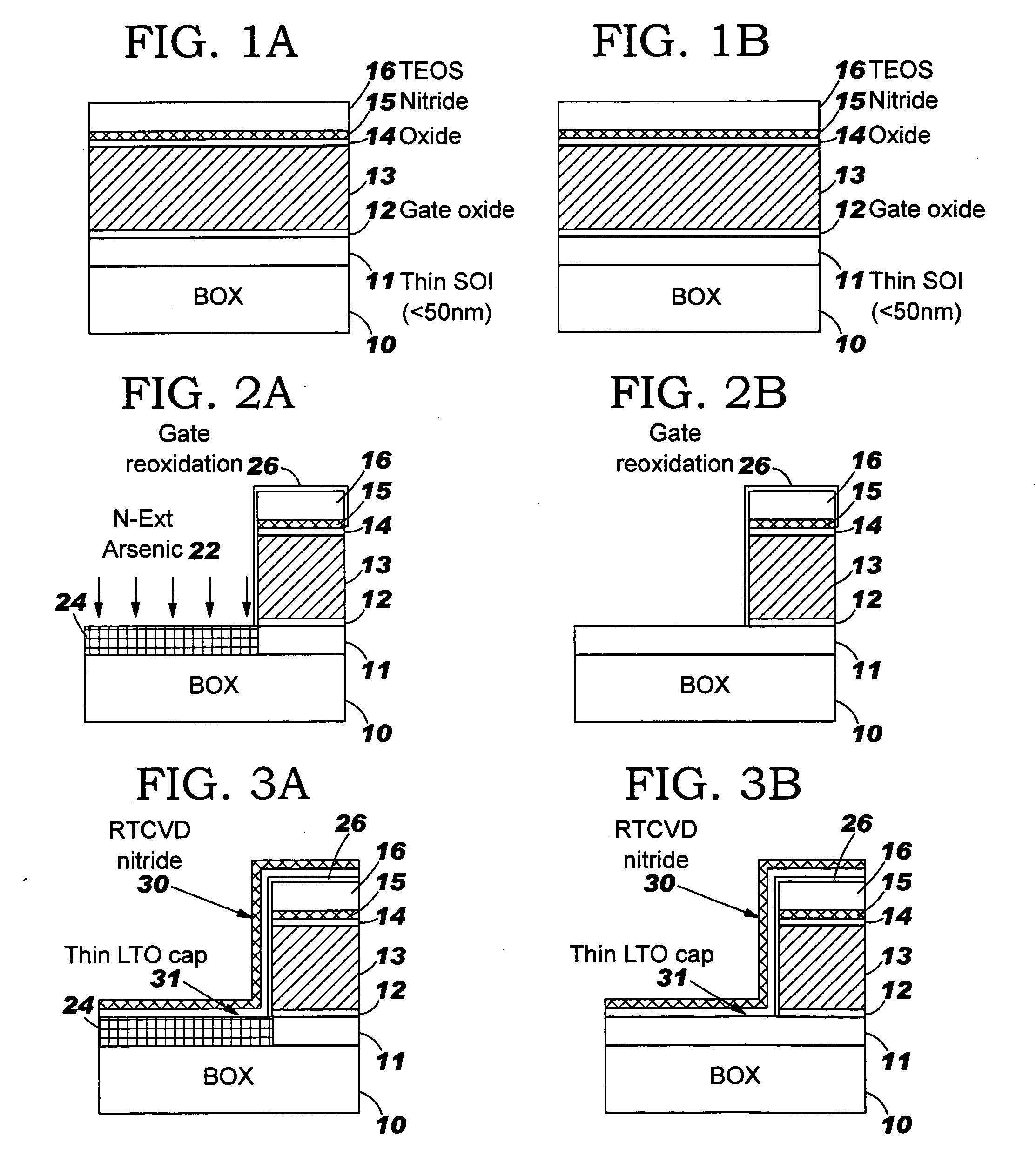
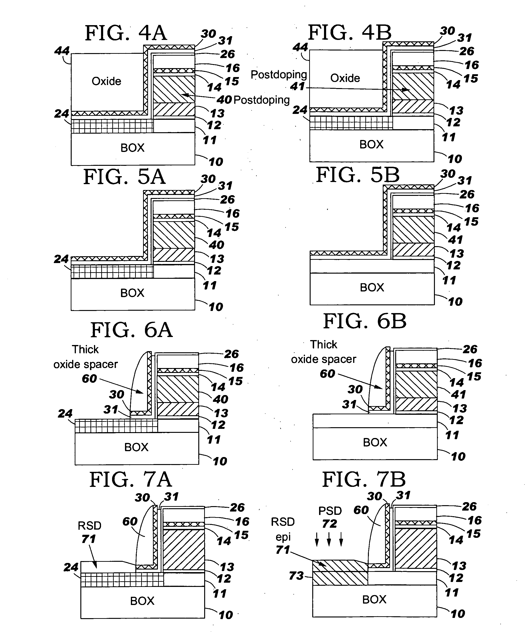
[0029] The invention presents a novel method of scaling down dimensions of all the electrodes in CMOS devices on SOI, including gate height. The invention resolves the problems associated with gate height reduction by providing a sacrificial layer above the gate poly. The buffer layer on top of the gate polysilicon artificially increases the gate height during the subsequent process integration, thereby making it possible to perform source, drain, and halo implantation at an energy high enough to sufficiently dope the source / drain and channel regions without incurring the problem of boron penetration through the poly gate and gate dielectric layer (as discussed above). In other words, the conventional self-aligned implantation process can be utilized with the invention because the thickness of the buffer layer causes the impurities to be implanted to the same depth within the inventive device structure including the source / drain and halo junctions and sidewall spacer size, as they w...


PUM


Abstract

Disclosed is a method and system of forming an integrated circuit transistor having a reduced gate height that forms a laminated structure having a substrate, a gate conductor above the substrate, and at least one sacrificial layer above the gate conductor. The process patterns the laminated structure into at least one gate stack extending from the substrate, forms spacers adjacent to the gate stack, dopes regions of the substrate not protected by the spacers to form source and drain regions adjacent the gate stack, and removes the spacers and the sacrificial layer.

Description

BACKGROUND OF INVENTION [0001] The present invention generally relates to integrated circuit transistors and more particularly to an improved structure and method that reduces the height of the gate electrode and simultaneously confines active dopants within each electrode, thereby maximizing integrated circuit performance. [0002] Challenges are encountered during conventional processing of high-performance complementary metal oxide semiconductor (CMOS) devices. As the feature size of transistors is scaled down, it is not only the size of electrodes (source, drain, and gate), but also the distance between them that becomes smaller, as they are formed closer to each other. The closer proximity increases electric field between the electrodes during operation of the device. For the overall integrated circuit performance, therefore, it becomes more and more critical to minimize parasitic capacitance between the electrodes, and at the same time, to maximize the drive currents without inc...

Claims


Application Information

Patent Timeline
IPC IPC(8): H01L21/336H01L21/84H01L27/12H01L29/423H01L29/45H01L29/49H01L29/786
CPCH01L21/84H01L29/458H01L29/6653H01L29/78621H01L29/66628H01L29/66772H01L29/6656H01L29/42376
Inventor PARK, HEEMYOUNGAGNELLO, PAUL D.GILBERT, PERCY V.LEE, BYOUNG H.O'NEIL, PATRICIA A.SHAHIDI, GHAVAM G.WELSER, JEFFREY J.
Owner GLOBALFOUNDRIES INC
Why Eureka
Try Eureka