Solder ball bonding method and bonding device

a solder ball and bonding device technology, applied in the direction of soldering apparatus, manufacturing tools, maintaining head carrier alignment, etc., can solve the problems of solder ball loading on the electrode b>9/b>, solder ball b>4/b> shifting position, etc., to achieve the effect of increasing the efficiency of bonding processing

Active Publication Date: 2005-03-10
SAE MAGNETICS H K LTD 50
View PDF5 Cites 12 Cited by
  • Summary
  • Abstract
  • Description
  • Claims
  • Application Information

AI Technical Summary

Benefits of technology

[0017] In consideration of the conventional problems described above, an object of the present invention is to provide a solder ball bonding method and a solder ball bonding device that can prevent solder balls from moving on a bonding portion, and can increase the efficiency of bonding processing, without applying an external force to a bonding object.

Problems solved by technology

However, problems such as those described below exist with the solder ball bonding devices mentioned above.
There is a problem in that the number of device configuring members increases.
Therefore, there is a danger that the solder ball 4 loaded onto the electrode 9 will shift position due to an external disturbance.
Accordingly, there is a problem in that additional means of holding the solder ball 4 has to be provided in addition to a manufactured product itself and the bonding device.
For cases in which a plurality of electrodes exist, the series of processes described above must be repeated for each of the plurality of electrodes, and it is difficult to increase the efficiency of the manufacturing processes.
In addition, although it is possible to arrange a plurality of solder balls in a plurality of holes with the devices having the three-layer structure made from the arrangement mask, the shutter mask, and the supply mask, bonding cannot be performed by conveying isolated specific solder balls to specific locations.

Method used


Image

  • Solder ball bonding method and bonding device
  • Solder ball bonding method and bonding device
  • Solder ball bonding method and bonding device

Examples


Embodiment Construction

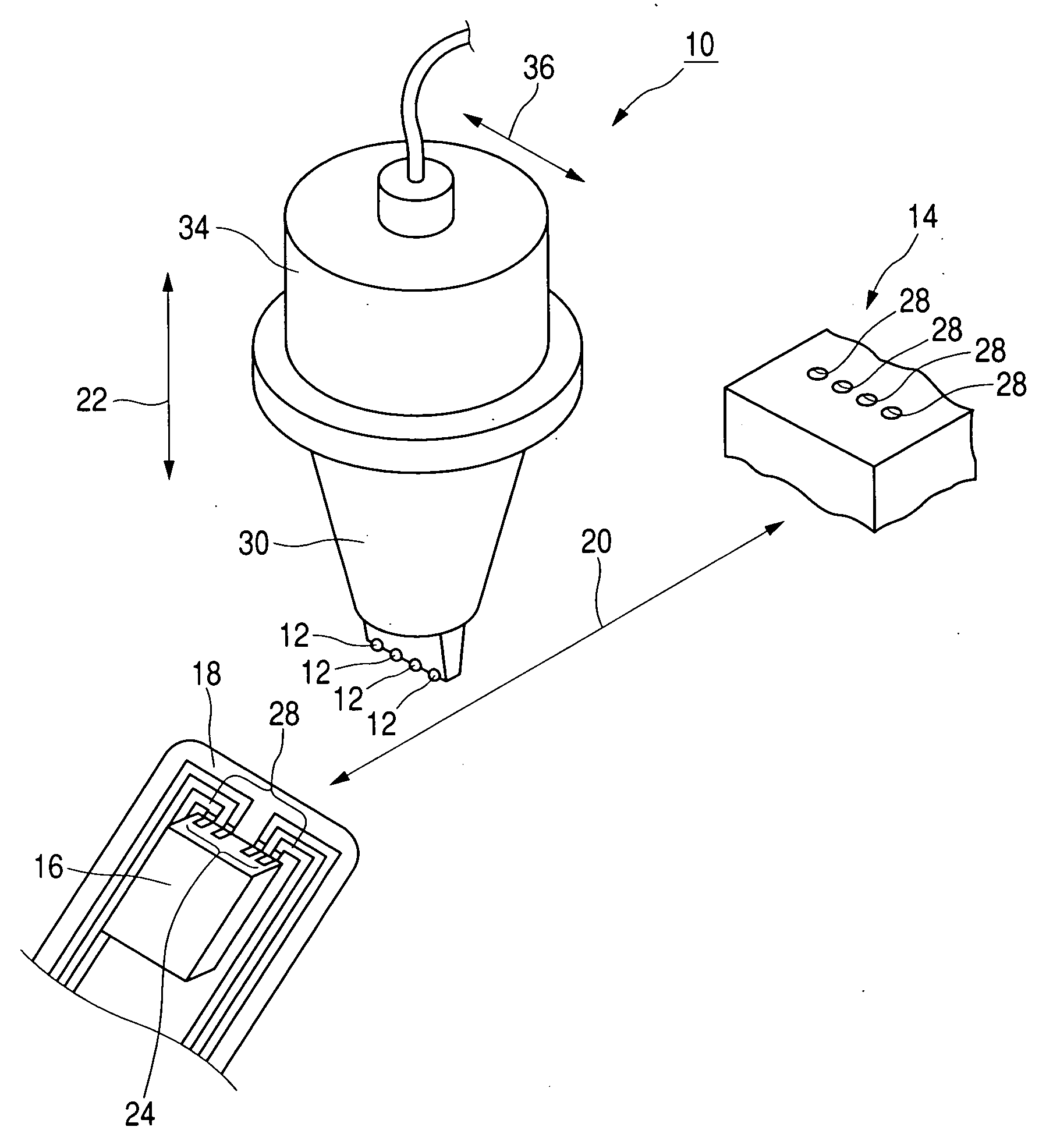
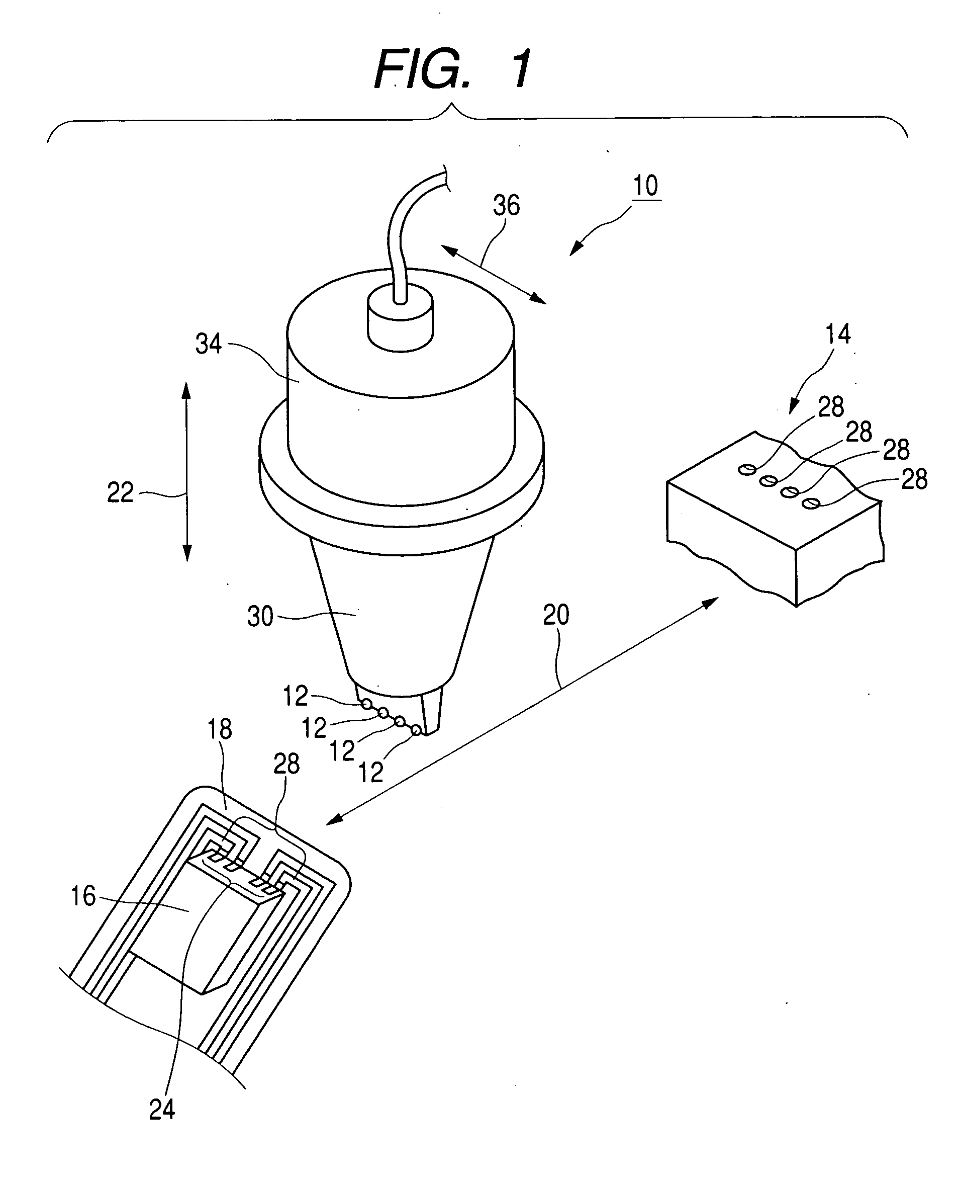
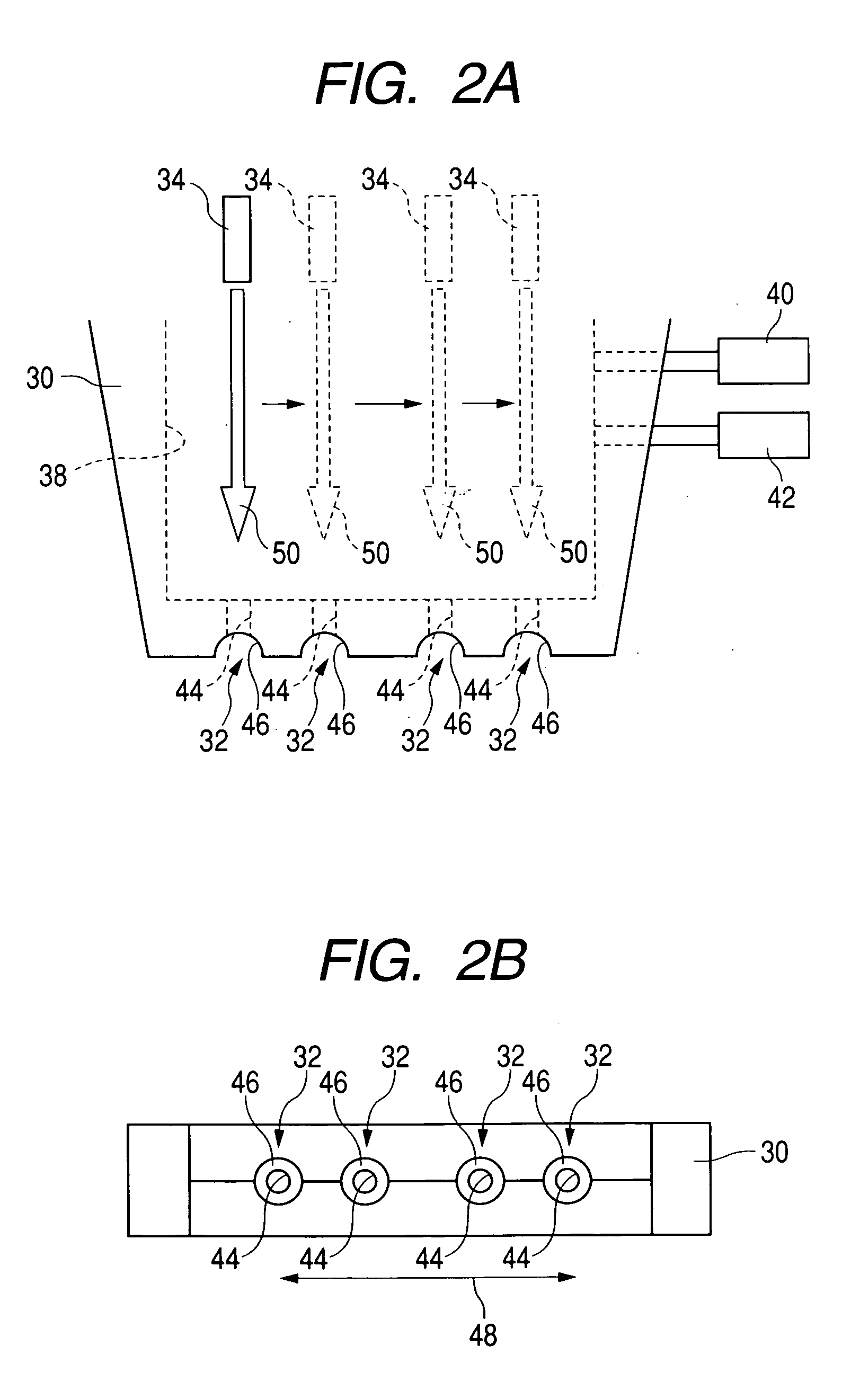
[0060] Specific preferred embodiments of a solder ball bonding method and a solder ball bonding device relating to the present invention are described below with reference to the drawings. FIG. 1 is a perspective view that shows an entire solder ball bonding device according to this embodiment. Referring to FIG. 1, a solder ball bonding device 10 according to this embodiment is made possible to move reciprocatively between a supplying device 14 that supplies solder balls 12 and structural parts of a magnetic head to be bonded (that is, a slider 16 in which GMR elements or the like are embedded, and a flexure 18 that supports the slider 16) by a moving means (not shown). It should be noted that the moving means can move in the directions of an arrow 20 and an arrow 22 in FIG. 1. Motion between the supplying device 14 and the structural parts of the magnetic head is achieved by combining the directions shown by the arrow 20 and the arrow 22. Further, image recognizing means that opera...


PUM

PropertyMeasurementUnit
outer diameteraaaaaaaaaa
pressureaaaaaaaaaa
structureaaaaaaaaaa

Abstract

Provided are a solder ball bonding method and a solder ball bonding device for performing bonding of a plurality of electrode portions formed on objects to be bonded by melting solder balls. The solder balls are suctioned by using a plurality of suction nozzles that follow the electrode portions of the objects to be bonded, and conveyed onto the electrode portions. A laser irradiation portion that is positioned above the suction nozzles is then moved in a direction along which the suction nozzles are arranged, while the solder balls are irradiated with laser light passing through suction openings of the suction nozzles by using the laser irradiation portion. Accordingly, it is possible to melt the plurality of solder balls on the electrode portions by using only a single laser irradiation portion.

Description

BACKGROUND OF THE INVENTION [0001] 1. Field of the Invention [0002] The present invention relates to a solder ball bonding method and a solder ball bonding device. In particular, the present invention relates to a solder ball bonding method and a solder ball bonding device that are suited for making fine bonding, such as bonding between a bonding pad that is formed on a magnetic head slider and a pad that is formed on a lead frame side. [0003] 2. Related Background Art [0004] A connection method is conventionally known, with which electrodes that are objects to be bonded are placed close to each other, the electrodes are made to contact ball-shaped solder (hereinafter called solder ball), and heat and ultrasonic vibration are applied to the solder ball (so-called ultrasonic pressure welding), thus making an electrical connection between the electrodes. [0005] Further, in addition to bonding by using pressure welding, a bonding method is also known in which a solder ball is disposed ...

Claims


Application Information

Patent Timeline
Patent Type & Authority Applications(United States)
IPC IPC(8): B23K1/00B23K1/005B23K3/00B23K3/06B23K31/02B23K101/36G11B5/60G11B21/21H01L21/60H05K3/34
CPCB23K1/0016B23K1/0056B23K3/0623B23K2201/36H05K3/3442H05K3/3478H01L2224/742H05K2203/0195H05K2203/041H05K2203/082H05K2203/107H01L2224/11003H01L2224/11334H05K3/3494B23K2101/36
Inventor SHINDO, OSAMUMIZUNO, TORUANDOH, YOUICHIYAMAGUCHI, SATOSHI
Owner SAE MAGNETICS H K LTD 50
Why Eureka
Try Eureka