

Semiconductor device, method of manufacturing the same and liquid jet apparatus
a technology of semiconductor devices and liquid jets, applied in the direction of printing, inking apparatus, transistors, etc., can solve the problems of wasteful current consumption, inability to satisfy the breakdown voltage required, and inability to obtain the current necessary to drive the electro-thermal converter, etc., to achieve high breakdown voltage, energy saving, and large current flow
- Summary
- Abstract
- Description
- Claims
- Application Information
AI Technical Summary
Benefits of technology
Problems solved by technology
Method used
Image

Examples
first embodiment
[0146] (First Embodiment)
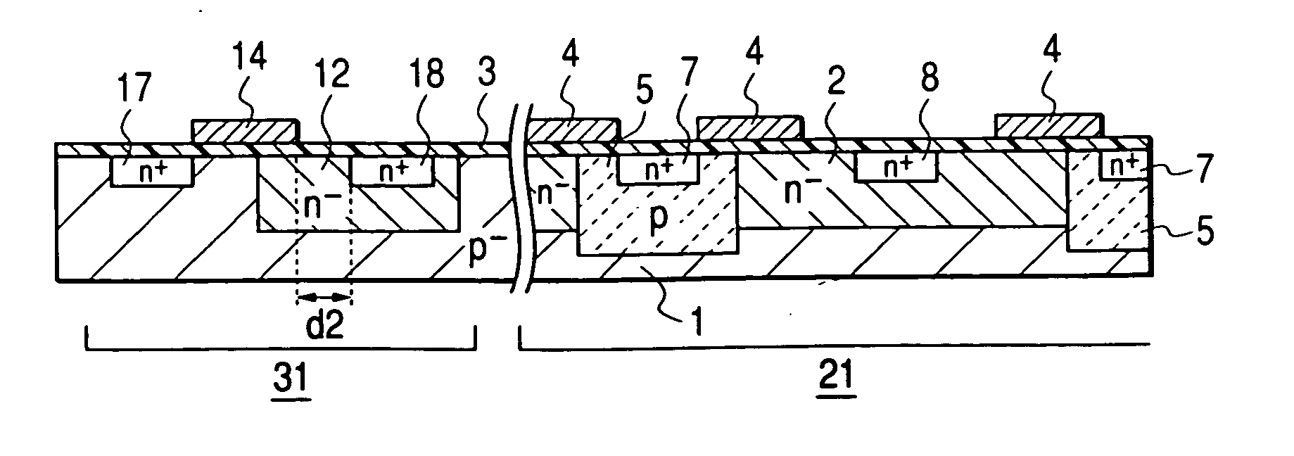
[0147] Next, a first embodiment of the present invention will be described with reference to the accompanying drawings. The cross-sectional structures of the switching element and the drive circuit element are identical with those shown in FIGS. 1A and 1B.
[0148] Reference numeral 1 denotes a semiconductor substrate of a first conductive type, 2 is a well region which is a first semiconductor region of a second conductive type, 3 is a gate insulating film, 4 is a gate electrode, 5 is a base region which is a second semiconductor region of a first conductive type, 7 is a source region that is aligned with the left end portion of the gate electrode, and 8 is a highly doped drain region which is formed apart from an end portion of a pn junction between the well region and the base region to the right hand side in the drawing, and is also laterally apart from the gate electrode.
[0149] The DMOS transistor 20 shown in FIG. 1A forms the base region 5 within the we...
second embodiment
[0175] (Second Embodiment)
[0176] This embodiment modifies the structure of the DMOS transistor that constitutes the switching element in the above-mentioned embodiment. Structures other than this are identical with those in the above-mentioned embodiment.
[0177]FIG. 8 shows a cross-section of a portion of a switching element array. In the DMOS transistor 21 used in this embodiment, the base region 5 is formed deeply so as to reach the p-type region of the substrate, in order to completely isolate the well region 2 in a lateral direction. With this structure, the drains of the respective segments can be electrically isolated from each other.
[0178] Therefore, since a dedicated element separation region is not required between the adjacent units as in the structure of FIG. 3, an occupied area is small, and the degree of freedom of a design when connecting the MDOS transistors in parallel with each other is also high.
[0179]FIGS. 9A, 9B, 9C, 9D and 9E are cross-sectional views for expl...
third embodiment
[0188] (Third Embodiment)
[0189] Next, another embodiment of the present invention will be described with reference to the accompanying drawings. FIGS. 10A and 10B are cross-sectional structural views of the switching element and the drive circuit element in accordance with the present invention, respectively, and FIGS. 11A, 11B, 11C and 11D are schematic views for explaining a process of manufacturing these elements.
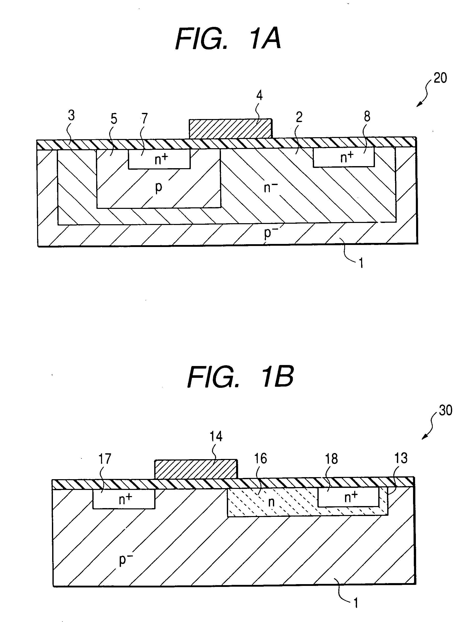
[0190]FIG. 10A shows an example of the switching element used in the present invention, which is identical in structure with that shown in FIG. 1A.
[0191]FIG. 10B shows elements contained in the circuit for driving the switching element shown in FIG. 10A, in which reference numeral 1 denotes a semiconductor substrate of a first conductive type, 12 is a well region that is a first semiconductor region of a second conductive type, 13 is a gate insulating film, 14 is a gate electrode, 17 is a source region aligned with the left end portion of the gate electrode, and 18 is ...
PUM
 Abstract
Description
Claims
Application Information