Optical system for detecting anomalies and/or features of surfaces

Active Publication Date: 2005-03-10
KLA TENCOR TECH CORP
View PDF25 Cites 47 Cited by
  • Summary
  • Abstract
  • Description
  • Claims
  • Application Information

AI Technical Summary

Benefits of technology

[0012] Radiation scattered or reflected from the first line and/or illuminated area is collected and the radiation collected from a portion of the line and/or illuminated area is focused to a corresponding detector in the array. In other words, each portion of the line is imaged onto a corresponding detector in the array. Since the line has a small dimension across its width, the detection sensitivity of the system is enhanced in a direction transverse (e.g. perpendicular) to the line. Preferably the dimension of the detector in the direction along the line is also chosen to be small, so that the resulting resolution of the detection system is the result of the dimensions of the width of the line in one dimension and the size of the detector in the other dimension, so that the system can be designed to have high detection sensitivity. On the other hand, since an entire line area of the surface is illuminated simultaneously, the system has higher throughput compared to dark field systems where an illuminated

Problems solved by technology

Such system requires significant time to image the entire surface of a photomask or semiconductor wafer because of the data rate required for imaging.
This greatly reduces the amount of photons originating from the source that reach the detector, and therefore reduces the sensitivity of bright field inspection.
Spot-scanning dark-field systems generally have higher inspection speed than bright-field systems, but with lower image resolution, and suffer some signal noise resulting

Method used


Image

  • Optical system for detecting anomalies and/or features of surfaces
  • Optical system for detecting anomalies and/or features of surfaces
  • Optical system for detecting anomalies and/or features of surfaces

Examples


Embodiment Construction

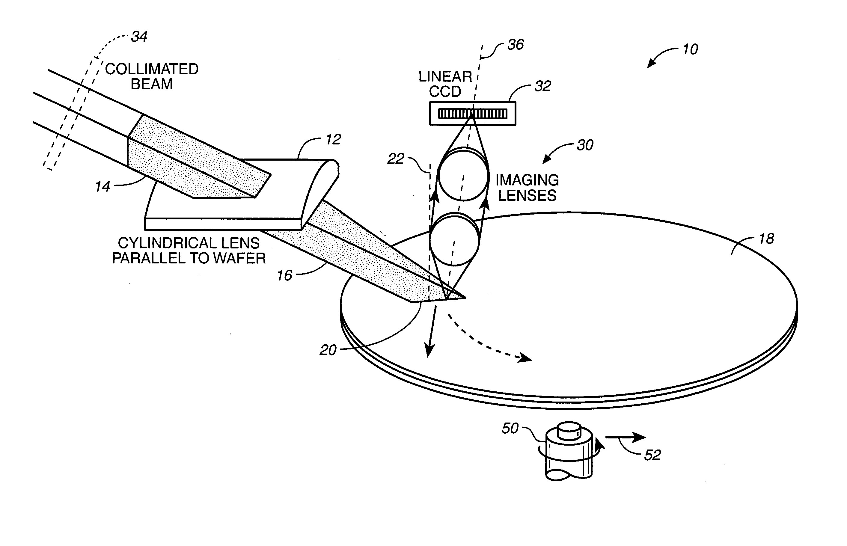
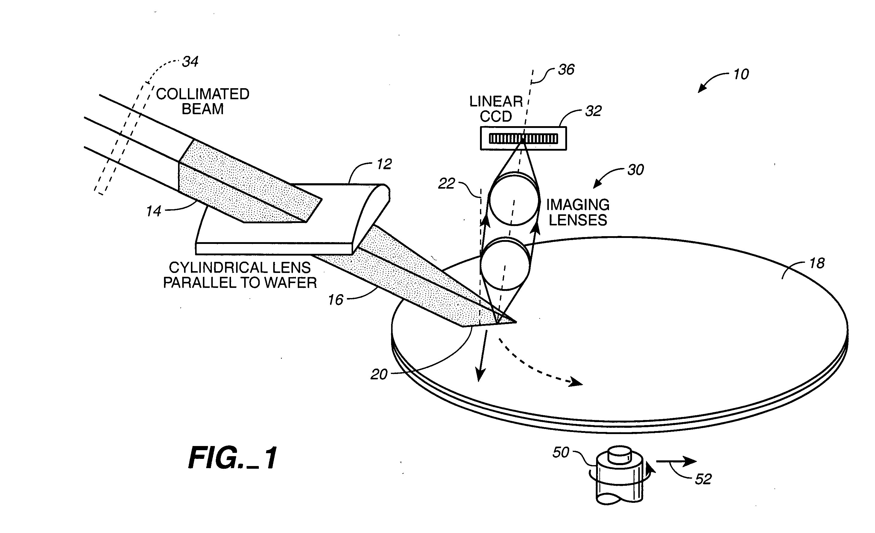
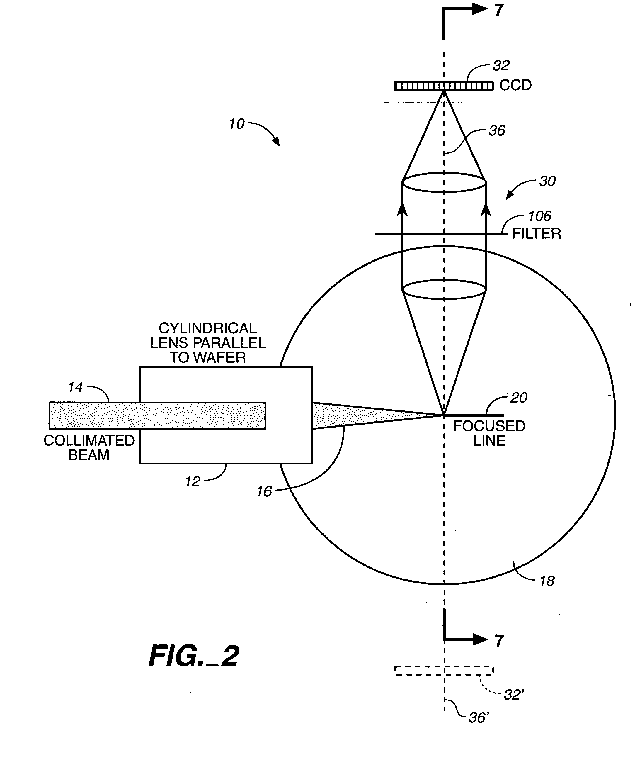
[0040] Bright-field image capability may be defined as using illumination from within the collection cone of the imaging optics, including laser-illuminated bright-field imaging. Dark-field image capability may be defined as using illumination from outside the collection cone of the imaging optics but within a plane containing the illumination axis and the axis normal to the wafer surface. Double-dark-field image capability may be defined as using illumination from outside the collection cone of the imaging optics and an imaging axis (of the imaging optics) which lies outside a plane containing the illumination axis and the axis normal to the wafer surface. Near-angle-dark-field image capability may be defined as using illumination incident near to the collection cone of the imaging optics or within the collection cone of the imaging optics but with the specular reflection from the wafer surface blocked.

[0041] The description below in reference to FIGS. 1-8 is mostly taken from the...


PUM


Abstract

A surface inspection of the system applies a first oblique illumination beam and may also apply a second illumination beam to illuminate a surface either sequentially or simultaneously. Radiation reflected or scattered is collected by preferably three collection channels and detected by three corresponding detector arrays, although a different number of channels and detector arrays may be used. One or both illumination beams are focused to a line on the surface to be inspected and each line is imaged onto one or more detector arrays in the up to three or more detection and collection channels. Relative motion is caused between the lines and the surface inspected in a direction perpendicular to the lines, thereby increasing throughput while retaining high resolution and sensitivity. The same detection channels may be employed by detecting scattered or reflected radiation from both illumination beams. Fourier filters may be employed to filter out diffraction at one or more different spatial frequencies.

Description

CROSS-REFERENCE TO RELATED APPLICATION [0001] This application claims benefit of U.S. Provisional Application Ser. No. 60 / 482,539 filed Jun. 24, 2003, which is related to U.S. patent application Ser. No. 08 / 904,892 filed Aug. 1, 1997, entitled “SYSTEM FOR DETECTING ANOMALIES AND / OR FEATURES OF A SURFACE” by Guoheng Zhao, Stanley Stokowski, and Mehdi Vaez-Iravani, herein referred to as the “Related Application”. The Related Application is herein incorporated herein by reference in its entirely.BACKGROUND OF THE INVENTION [0002] This invention relates in general to surface inspection systems, and in particular, to an improved system for detecting anomalies and / or features of a surface. [0003] The size of semiconductor devices fabricated on silicon wafers has been continually reduced. The shrinking of semiconductor devices to smaller and smaller sizes has imposed a much more stringent requirement on the sensitivity of wafer or photomask inspection instruments which are called upon to d...

Claims


Application Information

Patent Timeline
IPC IPC(8): G01N21/47G01N21/88G01N21/94G01N21/95G01N21/956
CPCG01N21/474G01N21/8806G01N21/95623G01N21/9501G01N21/94G01N21/95G01N21/88
Inventor LEWIS, ISABELLAVAEZ-IRAVANI, MEHDI
Owner KLA TENCOR TECH CORP
Why Eureka
Try Eureka