Display device and manufacturing method of display device

a technology of display element and manufacturing method, which is applied in the direction of discharge tube/lamp details, discharge tube luminescnet screen, organic semiconductor device, etc., can solve the problems of reduced reliability, reduced luminance, dark spot, shrinkage, etc., and achieves the elimination of irregularities, high light transmittance, and the effect of preventing wiring defects

Inactive Publication Date: 2005-03-24
SEMICON ENERGY LAB CO LTD
View PDF27 Cites 81 Cited by
  • Summary
  • Abstract
  • Description
  • Claims
  • Application Information

AI Technical Summary

Benefits of technology

[0034] As for an active layer of a TFT, an amorphous semiconductor film, a semiconductor film having a crystalline structure, a compound semiconductor film having an amorphous structure, and the like can be arbitrarily used. Alternativly, the active layer of the TFT may be formed of a semiamorphous semiconductor film (also referred to as a microcrystalline semiconductor film) having an intermediate structure between an amorphous structure and a crystalline structure (including a single crystalline structure, and a polycrystalline structure). The semiamorphous semiconductor film has a third condition that is stable with respect to free energy, and includes a crystalline region having short-distance order and lattice distortion. Further, at least a part of the semiamorphous semiconductor film includes a crystal grain of from 0.5 nm to 20.0 nm in size, and Raman spectrum is shifted to a lower wavenumber than 520 cm−1. The diffraction peak of (111) and (220), which is believed to be originated in a crystalline silicon lattice, is observed in the semiamorphous semiconductor film by X-ray diffraction. Further, the semiamorphous semiconductor film is added with hydrogen or halogen of at least 1 atom % as a terminator for dangling bonds. The semiamorphous semiconductor film is formed by glow discharge decomposition with silicide gas (by plasma CVD). As for the silicide gas, Si2H6, SiH2Cl2, SiHCl3, SiCl4, SiF4, and the like can be used, besides SiH4. The silicide gas may also be diluted with H2 or a mixture of H2 and at least one rare gas selected from the group consisting of He, Ar, Kr, and Ne. The dilution ratio may be in the range of from 1:2 to 1:1,000. The pressure may be approximately in the range of from 0.1 Pa to 133 Pa. The power frequency is in the range of from 1 MHz to 120 MHz, preferably 13 MHz to 60 MHz. The substrate heating temperature may be set at 300° C. or less, preferably from 100° C. to 250° C. As for impurity elements contained in the film, each concentration of impurities in atmospheric constituents such as oxygen, nitrogen, and carbon is preferably set at 1×1020 cm−1 or less. In particular, the oxygen concentration is set at 5×10¹⁹ atoms / cm3 or less; more preferably, 1×10¹⁹ atoms / cm3 or less. The electric field effect mobility μ of the TFT using the semiamorphous semiconductor film as the active layer is in the range of from 1 cm 2 / Vsec to 10 cm2 / Vsec.
[0035] According to a heat resistant planarizing film of the invention, wiring defects of a display element can be prevented by eliminating irregularities due to a gate electrode or a semiconductor layer in a display device forming a TFT. The heat resistant planarizing film of the invention can have high light transmittance and preferable display properties.
[0036] In addition, in a light emitting display device using a layer containing an organic compound as a light emitting layer; the reliability can be improved by providing an interlayer insulating film which has the small amount of dehydration and degasification.
[0037] By using a structure of the display device according to the invention, the number of steps is simplified and display devices can be manufactured with higher yield and at lower cost.

Problems solved by technology

In the display device (panel) using the above light emitting element, the moisture which enters inside leads a serious decrease in reliability, and a dark spot, shrink, and reduction in luminance from a peripheral part of a display device.

Method used


Image

  • Display device and manufacturing method of display device
  • Display device and manufacturing method of display device
  • Display device and manufacturing method of display device

Examples


embodiment 1

[0116] Embodiment 1

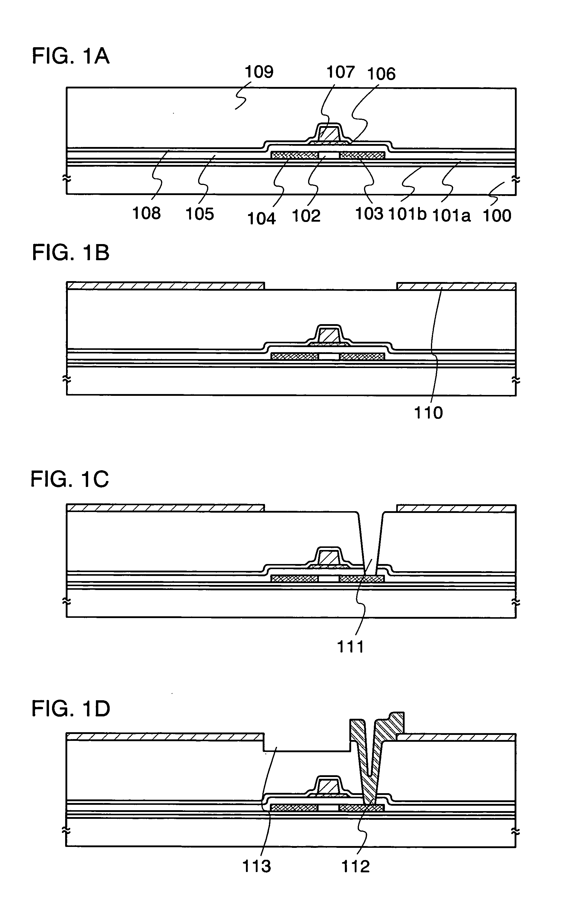
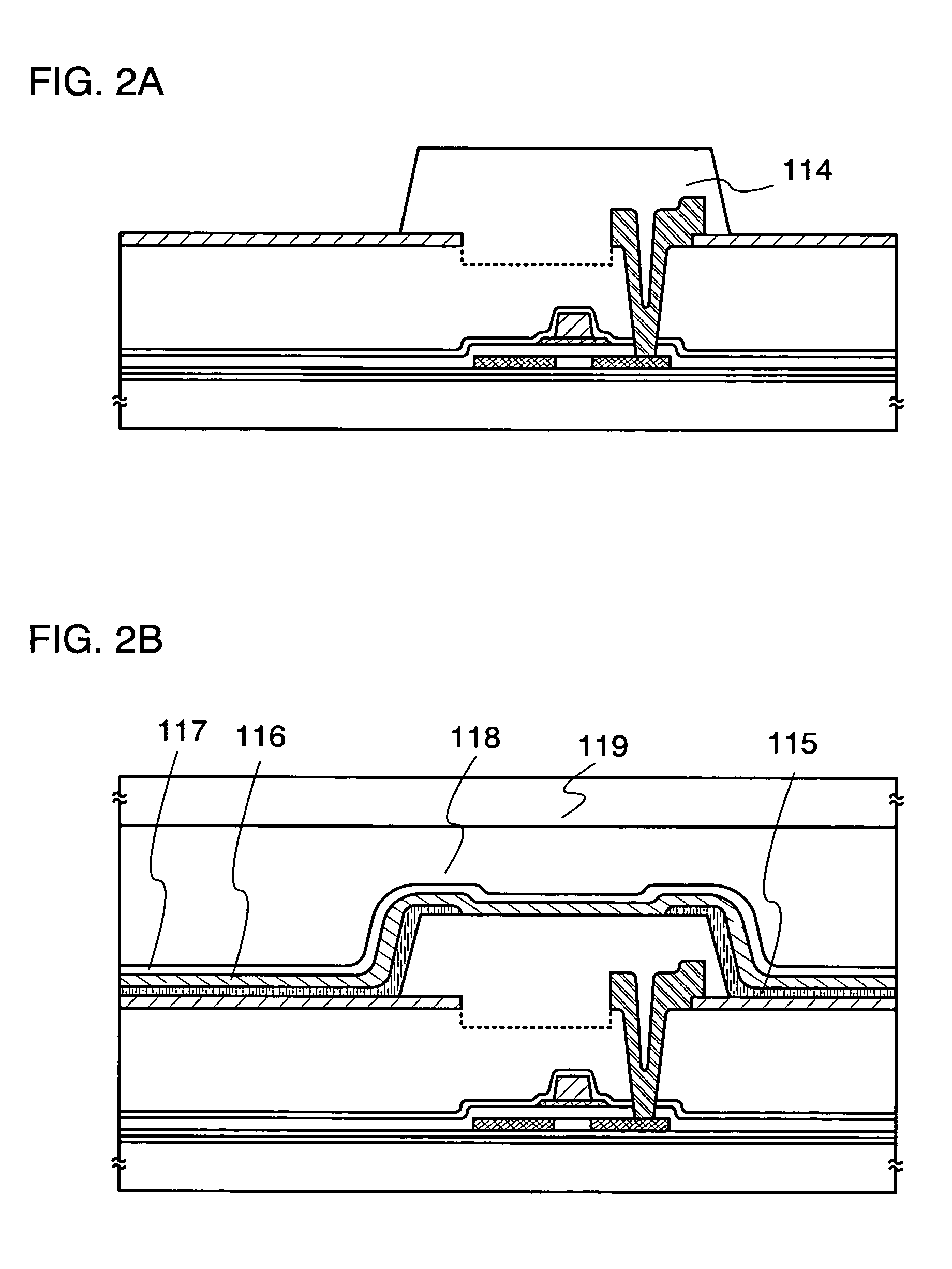
[0117] In this embodiment, a manufacturing method of the display device described in Embodiment Mode will be explained with reference to FIGS. 1A to 1D and FIG. 14.

[0118] A 50-nm-thick a silicon nitride oxide film and a 100-nm-thick a silicon oxynitride film are formed over a substrate 100 as a base film 101 by plasma CVD.

[0119] Next, a semiconductor film is formed on the base film. In this embodiment, an amorphous silicon film is formed to a thickness of 54 nm by plasma CVD. In this embodiment, thermal crystallization or laser crystallization method using a metal element which promotes crystallization is performed to the amorphous silicon film.

[0120] Nickel is used as the metal element, and is doped into the amorphous silicon film by solution coating. A method for doing the metal element into the amorphous silicon film, a method using a solution is simple and easily performed, and is useful for easily adjusting concentration of the metal element. At this time,...

embodiment 2

[0157] Embodiment 2

[0158] In this embodiment, examples of top emission type and dual emission type light emitting display devices manufactured according to Embodiment 1 will be described with reference to FIG. 5 and FIG. 9.

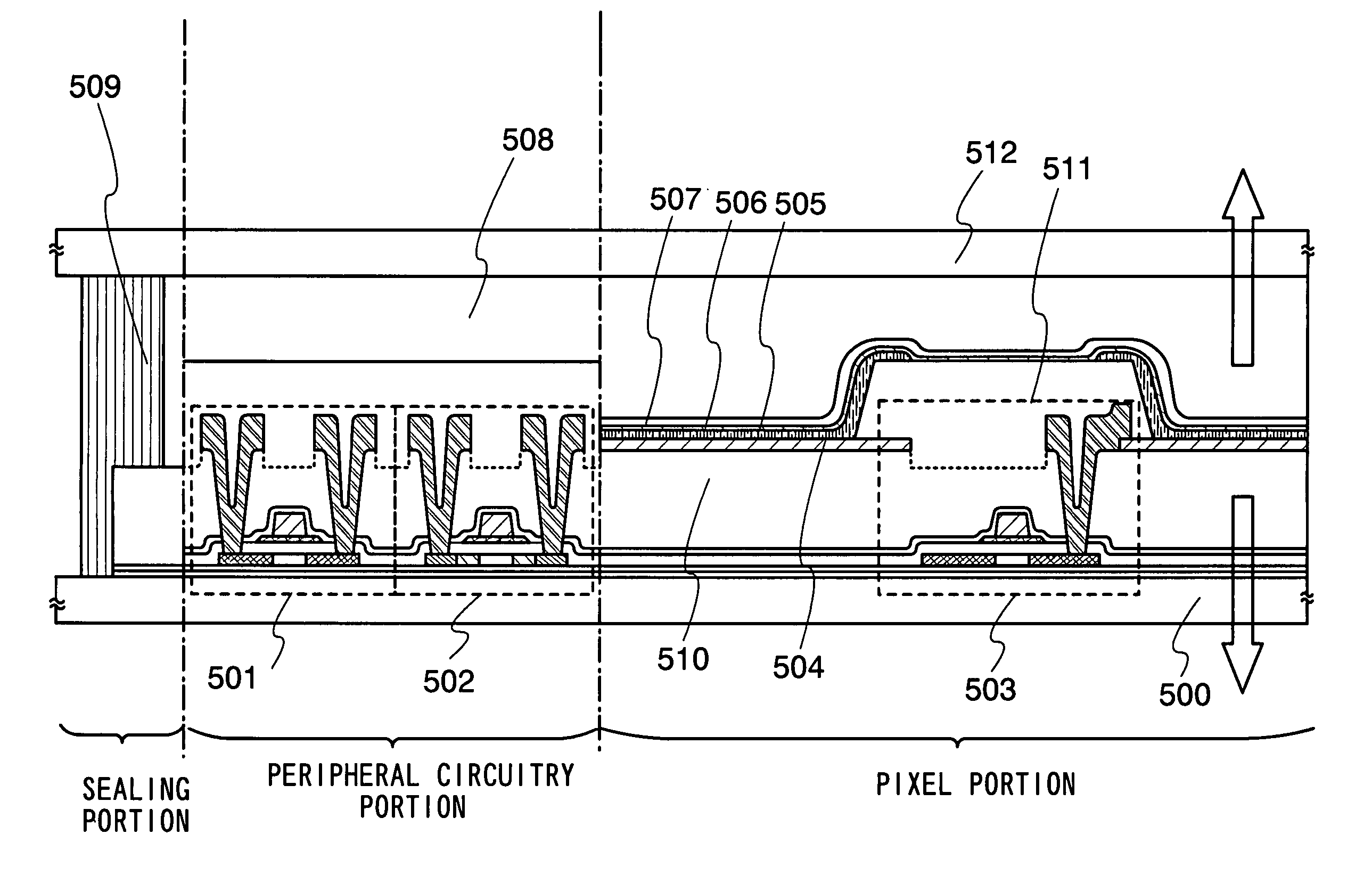
[0159] In FIG. 5, reference numeral 500 denotes a substrate, 501, 502, and 503 denote TFTs, 504 denotes a pixel electrode, 505 denotes a light emitting layer, 506 denotes an electrode, 507 denotes a transparent conductive film, 508 denotes a filler, 509 denotes a sealant, 510 denotes a heat-resistant planarizing film, 511 denotes a partition wall, and 512 denotes a sealing substrate.

[0160] A light emitting display device in FIG. 5 is a dual emission type, which has a structure in which light is emitted from both top and bottom surfaces in the directions of arrows. In this embodiment, a transparent conducive film is formed and etched to the desired shape to form the pixel electrode 504. A conductive film formed by mixing 2% to 20% of zinc oxide (ZnO) into indium ...

embodiment 3

[0167] Embodiment 3

[0168] In this embodiment, an example of an inverted staggered TFT will be described with reference to FIG. 6 and FIG. 7. Parts aside from the TFT is similar to FIG. 5 described in Embodiment Mode; the detailed description thereof is omitted here.

[0169]FIG. 6 shows a channel stop type TFT. Reference numeral 600 denotes a substrate, 601 and 602 denote TFTs of a driver circuit area. A gate insulating film 604, a semiconductor layer 605 formed with an amorphous semiconductor film, an n+ layer 607, and a metal layer 608 are formed over a gate electrode 603. A channel stopper 606 is formed above an area which will become a channel region of the semiconductor layer 605. A source or drain electrode 611 is formed. Reference numeral 609 denotes an insulating film, 612 denotes a first electrode, 613 denotes a light emitting layer, 614 denotes a second electrode, 616 denotes a passivation film, 619 denotes a filler, 618 denotes a sealant, 610 denotes a heat-resistant planar...


PUM


Abstract

It is an object of the present invention to provide a reliable display device and a method for manufacturing the display device reducing the number of manufacturing steps, and with higher yield. A display device according to the invention includes a plurality of display elements each having a first electrode, a layer containing an organic compound, and a second electrode. The display device further includes a heat-resistant planarizing film over a substrate having an insulating surface, a first electrode over the heat-resistant planarizing film, a wiring covering an end portion of the first electrode, a partition wall covering the end portion of first electrode and the wiring, a layer containing an organic compound, and a second electrode over the layer containing an organic compound.

Description

BACKGROUND OF THE INVENTION [0001] 1. Field of the Invention [0002] The invention relates to a display device having an element in which a light emitting material is sandwiched between electrodes (hereinafter referred to as a light emitting element). [0003] 2. Description of the Related Art [0004] Recently, the development of a liquid crystal display device and an electroluminescent display device in which thin film transistors (TFTs) are integrated over a glass substrate has been in progress. As to each of such display devices, TFTs are manufactured over a glass substrate by thin film formation technologies, and a liquid crystal element or a light emitting element (electroluminescent (hereinafter simply referred to as EL) element) formed over various circuits configured with the thin film transistors, thus functions as a display device. [0005] A circuit formed with TFTs has some surface irregularities, hence in forming the liquid crystal elements or the light emitting elements over...

Claims


Application Information

Patent Timeline
Patent Type & Authority Applications(United States)
IPC IPC(8): H01J1/62H01L21/336H01L21/77H01L27/12H01L27/32H01L51/52H05B33/02H05B33/10H05B33/12H05B33/22H05B44/00
CPCH01L27/12H01L27/1214H01L27/3246H01L27/3258H01L27/3276H01L27/3248H01L51/5206H01L51/5237H01L51/529H01L2251/5315H01L2251/5323H01L29/66757H10K59/123H10K59/124H10K59/122H10K59/131H10K50/81H10K50/87H10K50/8426H10K2102/3031H10K2102/3026
Inventor YAMAZAKI, SHUNPEISAKAKURA, MASAYUKINAGAI, MASAHARUMATSUDA, YUTAKAAKIMOTO, KENGOFUJII, GENYAMAGUCHI, TETSUJI
Owner SEMICON ENERGY LAB CO LTD
Why Eureka
Try Eureka