Semiconductor device and system

Active Publication Date: 2005-03-24
RENESAS ELECTRONICS CORP
View PDF1 Cites 10 Cited by
  • Summary
  • Abstract
  • Description
  • Claims
  • Application Information

AI Technical Summary

Benefits of technology

[0006]FIG. 16 shows a cross sectional view of an element structure examined by the present inventor as described above. In FIG. 16, a MOSFET 9 is used as a transfer MOSFET and an MB1 is shown as a MOSFET constituting the input circuit. In FIG. 16, reference symbols are defined as follows; SUB denotes a semiconductor substrate, W denotes a well, S denotes the source, D denotes the drain, and G denotes the gate of a MOS transistor. For example, the SUB, S, and

Problems solved by technology

In the case of the official gazette (1), however, the input circuit used for signal voltage conversion as described above has many elements, so that the circuit power consumption increases.
The input circuit is thus not considered to be practical so much.
In spite of this, when the input voltage is excessive

Method used


Image

  • Semiconductor device and system
  • Semiconductor device and system
  • Semiconductor device and system

Examples


Embodiment Construction

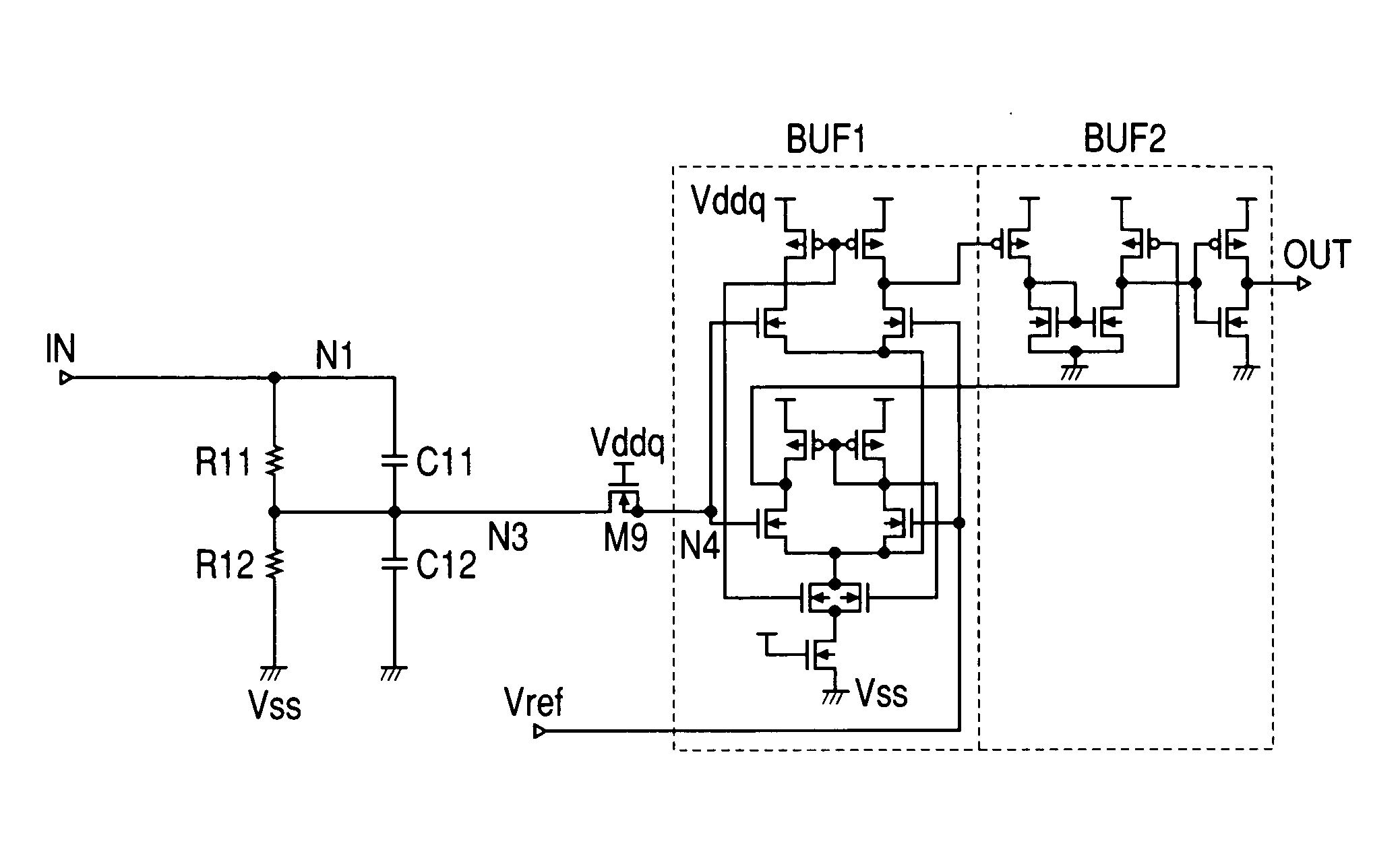
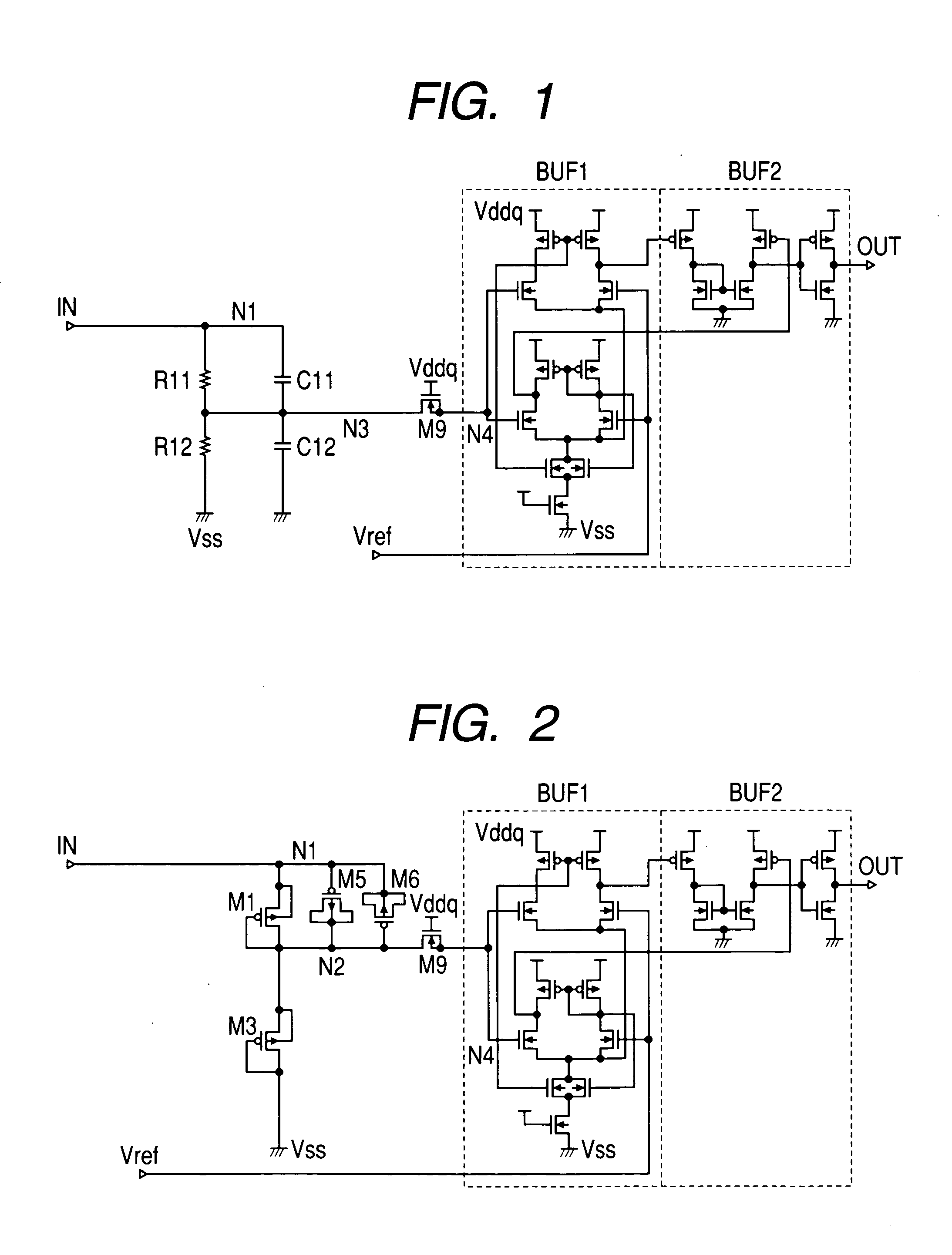
[0026]FIG. 1 shows a circuit diagram of an input circuit used in a semiconductor device in an embodiment of the present invention. Resistors R11 and R12 are connected to each other serially so as to constitute a voltage dividing circuit disposed between an input terminal IN and the ground potential of the input circuit. The resistance values of the resistors R11 and R12 are controlled so that a current flowing from the input terminal IN satisfies a predetermined standard. If a voltage dividing circuit is constituted so as to obtain such a large resistance value, transmission of input signals will be delayed due to, for example, the parasitic resistance, etc. added to the voltage dividing output node while the power consumption of the semiconductor device is reduced.

[0027] In this embodiment, therefore, to realize both reduction of the power consumption and quick operation of the semiconductor device, a capacitor C11 is connected to the resistor R11 in parallel. In other words, the ...


PUM


Abstract

Disclosed herewith is a semiconductor device improved to prevent withstand voltage defects that might occur in each MOSFET used therein and a system to be designed easily and prevented from withstand voltage defects that might occur in each semiconductor used therein. The system includes the first and second input circuits, each being constituted by MOSFETs manufactured in the same process. The first input circuit receives a voltage of a first signal inputted from a first external terminal and divided by first and second resistor means while the AC component of the input signal is transmitted to the input circuit through a capacitor disposed in parallel to the first resistor means. The second input circuit receives a second input signal inputted from a second external terminal and reduced in signal amplitude so as to become smaller than that of the first input signal. The system also includes a second semiconductor device corresponding to the first input circuit and a third semiconductor device corresponding to the second input circuit.

Description

BACKGROUND OF THE INVENTION [0001] The present invention relates to a semiconductor device and a system. More particularly, the present invention relates to a technique usable effectively for an input circuit in each LSI / IC used in a system constituted of a plurality of LSIs / ICs, each having an input / output interface corresponding to a signal voltage different from others. [0002] In an investigation of some well-known examples performed after the completion of the present invention, the present inventor et al have received a report of existence of official gazettes of (1) Japanese Unexamined Patent Publication No. Hei 5(1993)-266666 and (2) Japanese Unexamined Patent Publication No. 2001-251176 that are related to the present invention. The official gazette (1) discloses a semiconductor memory that can prevent transistors from destruction that might occur in the input circuit with use of an input amplitude limiting circuit disposed between an input terminal and the input circuit. Th...

Claims


Application Information

Patent Timeline
IPC IPC(8): H01L27/04H01L21/822H01L27/02H03K19/003H03K19/0175
CPCH01L27/0251H01L27/0259H01L2924/0002H03K19/00315H01L2924/00
Inventor NEGISHI, TAKEMINAMBU, HIROAKIKANETANI, KAZUOKAZAMA, HIDETO
Owner RENESAS ELECTRONICS CORP
Why Eureka
Try Eureka