
Preparation method of super junction power device

A technology of power devices and super junctions, which is applied in semiconductor/solid-state device manufacturing, semiconductor devices, electrical components, etc., can solve the problems of limited dopant concentration, limited etching depth and oxide film thickness, and electronic unevenness to achieve durability The effect of high voltage value, protection against damage, and low on-resistance

Active Publication Date: 2021-04-09
北京利宝生科技有限公司
View PDF0 Cites 0 Cited by
  • Summary
  • Abstract
  • Description
  • Claims
  • Application Information

AI Technical Summary

Problems solved by technology

However, the first type of manufacturing method has electron unevenness and diffusion, which limits the concentration of dopants; while in the second type of manufacturing method, the etching depth and oxide film thickness are also limited by the airflow intensity in the vertical direction; therefore, the existing The electrical performance of super junction power devices needs to be improved

Method used


Image

  • Preparation method of super junction power device
  • Preparation method of super junction power device
  • Preparation method of super junction power device

Examples


Embodiment Construction

[0050] In order to further explain the technical solution of the present invention, the present invention will be described in detail below through specific examples.

[0051] Such as Figure 1 to Figure 10 As shown, the present invention discloses a preparation method of a super junction power device, which comprises the following steps:

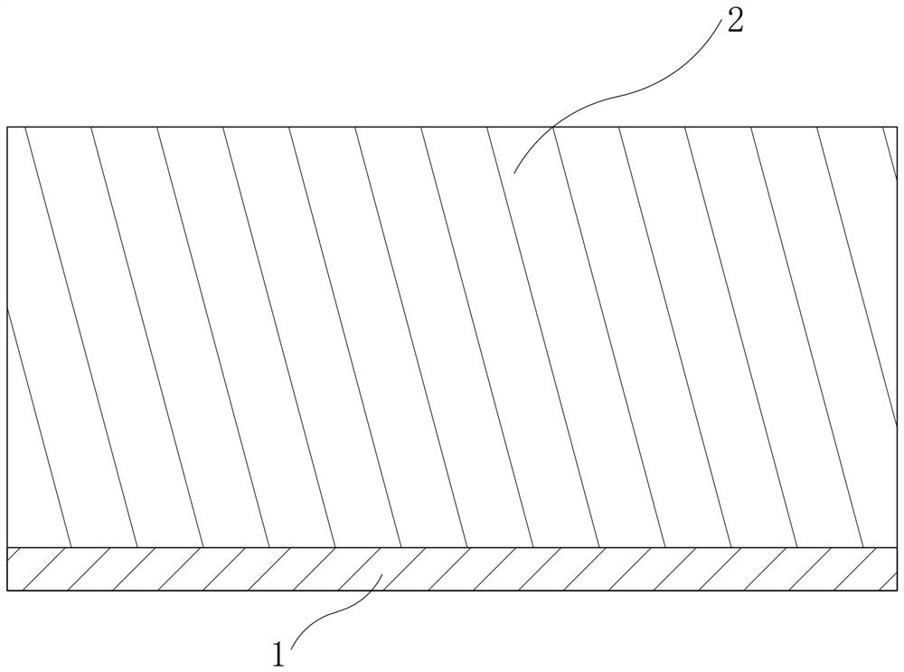
[0052] Step 1: Provide a semiconductor substrate 1 with a high doping concentration and an N-type conductivity type, and form a first epitaxial layer 2 with an N-type conductivity type on the front surface of the N-type semiconductor substrate 1;

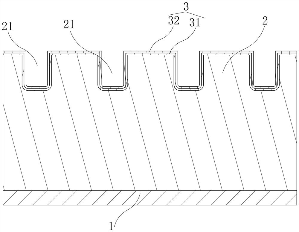
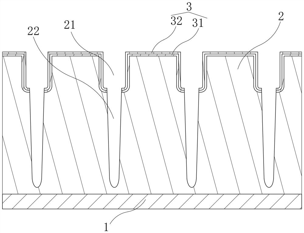
[0053] Step 2: Etch the front side of the first epitaxial layer 2 to form several gate trenches 21, and grow a protective layer 3 on the first epitaxial layer 2, the protective layer 3 covers the top surface of the first epitaxial layer 2 and each gate Pole trench 21; the protective layer 3 may include a basic protective layer 31 and a passivation layer 32 grown sequentially, and the basic prote...


PUM


Abstract

The invention discloses a preparation method of a super junction power device. According to the preparation method, dopant of a second epitaxial layer is diffused into a first epitaxial layer through a thermal diffusion process to obtain a super junction; With the preparation method of the invention adopted, the withstand voltage value of the super junction power device can be effectively improved, and the on-resistance is reduced.

Description

technical field [0001] The invention relates to the technical field of semiconductors, in particular to a preparation method of a super junction power device. Background technique [0002] Super junction power device is a new type of power semiconductor device with rapid development and wide application. It introduces the superjunction (SuperJunction) structure on the basis of ordinary double diffused metal oxide semiconductor (DMOS); in addition to having high input impedance of DMOS, fast switching speed, high operating frequency, easy voltage control, good thermal stability, and driving circuit In addition to being simple and easy to integrate, it also overcomes the disadvantage that the on-resistance of DMOS increases with the breakdown voltage to the power of 2.5. At present, super-junction DMOS has been widely used in power supplies or adapters for consumer electronics products such as personal computers, notebook computers, netbooks, mobile phones, lighting (high-pre...

Claims


Application Information

Patent Timeline
IPC IPC(8): H01L21/336H01L29/06H01L29/78
CPCH01L29/0634H01L29/0649H01L29/66825H01L29/66484H01L29/7841H01L29/7831H01L29/66734H01L29/7813
Inventor 金宰年叶宏伦钟其龙刘芝韧刘崇志
Owner 北京利宝生科技有限公司
Learn More