Method and apparatus for providing an antireflection coating on the output facet of a photonic integrated circuit (PIC) chip

a photonic integrated circuit and anti-reflection coating technology, applied in multiplex communication, semiconductor lasers, instruments, etc., can solve the problems of degrading channel signals, affecting the performance of the optical component, and introducing optical insertion losses for each optical component and fiber coupling

Inactive Publication Date: 2005-03-24
INFINERA CORP
View PDF78 Cites 40 Cited by
  • Summary
  • Abstract
  • Description
  • Claims
  • Application Information

AI Technical Summary

Problems solved by technology

Prior to this time, most long haul telecommunication networks were generally handled via electrical domain transmission, such as provided through wire cables, which is bandwidth limited.
Each of these device / fiber connections introduces a deleterious, backward reflection into the transmitter, which can degrade the channel signals.
Each optical component and fiber coupling also typically introduces an optical insertion loss.
Part of the cost of the optical transmitter is associated with the requirement that the optical components also be optically compatible.
Conventional optical fibers typically do not preserve optical polarization.
In order to attenuate the effects of polarization dispersion, the modulator and the optical combiner are, therefore, designed to be polarization insensitive, increasing their cost.
However, polarization preserving fibers are expensive and increase packaging costs since they require highly accurate angular alignment of the fiber at each coupling point to an optical component in order to preserve the initial polarization of the channel signal.
Increasing the number of channels requires precise control of channel assignment and more precise control over signal dispersion, which dramatically increases the complexity and cost of the fiber-optic components of the system.
A further complication is that many pre-existing optical networks use different types of optical fibers in the different optical links of the optical network having, therefore, different dispersion effects over different fiber lengths.
In some cases, the wavelengths of the optical channels generated at the optical transmitter may not be optimal for one or more optical links of the optical span.

Method used


Image

  • Method and apparatus for providing an antireflection coating on the output facet of a photonic integrated circuit (PIC) chip
  • Method and apparatus for providing an antireflection coating on the output facet of a photonic integrated circuit (PIC) chip
  • Method and apparatus for providing an antireflection coating on the output facet of a photonic integrated circuit (PIC) chip

Examples


Embodiment Construction

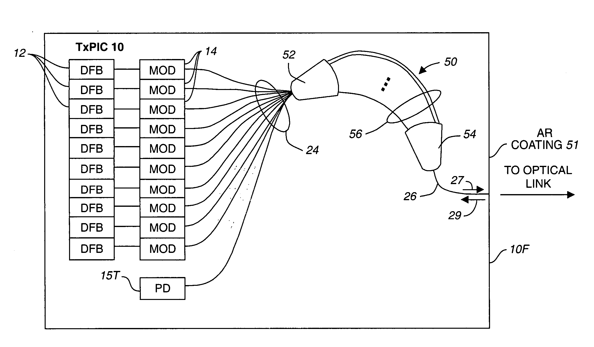
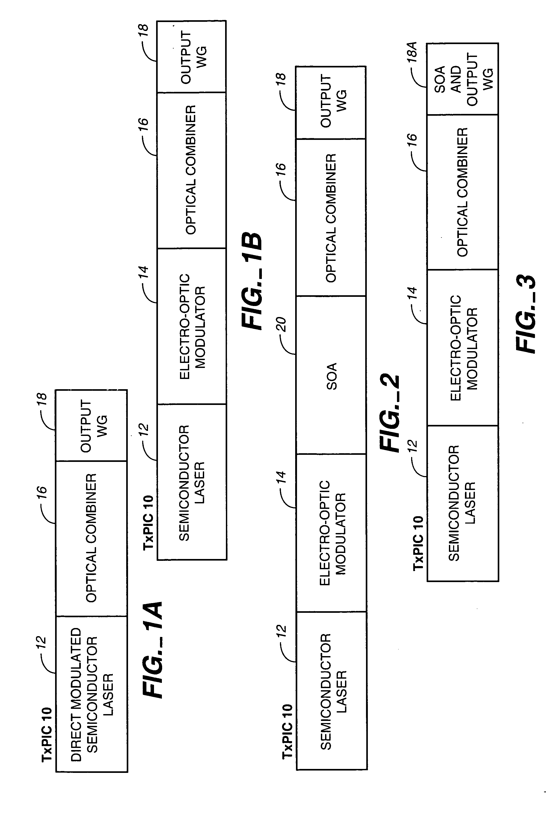
[0130] Reference is now made to FIGS. 1A and 1B which illustrate, in block form, an optical path on a monolithic TxPIC chip 10 showing plural active and passive optically coupled and integrated components. What is shown in diagrammatic form is one channel of such a chip. Both FIGS. 1A and 1B show modulated sources coupled to an optical combiner. Shown in FIG. 1A is one of an array of sources comprising a directly modulated semiconductor laser 12 integrated with an optical combiner 16 having an optical output waveguide 18 to take a combined channel signal off-chip. Shown in FIG. 1B is one of an array of sources comprising a semiconductor laser 12 optically coupled to one of an array of modulators comprising an electro-optic modulator 14 optically coupled to an input of an optical combiner 16 with the output of combiner 16 coupled to an optical output waveguide 18. There are plural optical paths on chip 10 of semiconductor laser 12 and electro-optic modulator 14, also in combination r...


PUM

PropertyMeasurementUnit
center wavelengthaaaaaaaaaa

Abstract

An on-chip photodiode is provided in a photonic integrated circuit (PIC) on a semiconductor chip to monitor or check for antireflection qualities of an AR coating applied to the front facet of the semiconductor chip.

Description

REFERENCE TO RELATED APPLICATION [0001] This application is division of patent application Ser. No. 10 / 317,935, filed Dec. 11, 2002, which is a continuation of patent application Ser. No. 10 / 267,331, filed Oct. 8, 2002, also published on May 22, 2003 as Publication No. US2003 / 0095737A1, which claims priority to the following provisional application Ser. No. 60 / 60 / 328,207, filed Oct. 9, 2001; Ser. No.: 60 / 328,332, filed Oct. 9, 2001; Ser. No. 60 / 370,345, filed Apr. 5, 2002; Ser. No. 60 / 378,010, filed May 10, 2002; Ser. No. 60 / 392,494, filed Jun. 28, 2002; and Ser. No. 60 / 367,595, filed Mar. 25, 2002, all of which applications are also assigned to a common assignee and are incorporated herein by their reference.BACKGROUND OF THE INVENTION [0002] 1. Field of the Invention [0003] This invention relates generally to optical telecommunication systems and more particularly to optical transport networks employed in such systems deploying photonic integrated circuits (PICs) for wavelength di...

Claims


Application Information

Patent Timeline
Patent Type & Authority Applications(United States)
IPC IPC(8): G02B6/12G02B6/34G02F1/017H01L31/12H01S3/00H01S3/13H01S5/00H01S5/026H01S5/0625H01S5/0683H01S5/12H01S5/20H01S5/22H01S5/34H01S5/40H01S5/50H04B10/00H04B10/04H04B10/145H04B10/17H04J14/02
CPCB82Y20/00H04J14/0276G01R31/318511G02B6/12004G02B6/12007G02B6/12011G02B6/12019G02B6/12021G02B6/12023G02B6/12026G02B6/12028G02B6/12033G02B6/131G02B6/136G02B6/4204G02F1/01725G02F2001/0175G02F2001/01758G02F2203/69H01L31/125H01S5/0014H01S5/0085H01S5/02248H01S5/026H01S5/0262H01S5/0264H01S5/0265H01S5/0268H01S5/06256H01S5/06258H01S5/0683H01S5/06832H01S5/12H01S5/1228H01S5/2077H01S5/22H01S5/3408H01S5/4031H01S5/4087H01S5/50H04B10/2914H04B10/50H04J14/02H04J14/0282H04J14/0246H04J14/025H04J14/0258H04J14/0265G01R31/31728G02F1/01758G02F1/0175H01S5/02325
Inventor JOYNER, CHARLES H.
Owner INFINERA CORP
Why Eureka
Try Eureka