Semiconductor light-emitting device

Active Publication Date: 2005-03-31
EPISTAR CORP
View PDF5 Cites 256 Cited by
  • Summary
  • Abstract
  • Description
  • Claims
  • Application Information

AI Technical Summary

Benefits of technology

The present invention has been proposed in order to solve the aforementioned problem, and an object of the present invention is to

Problems solved by technology

When an electrode is formed on a p-type nitride-based semiconduc

Method used


Image

  • Semiconductor light-emitting device
  • Semiconductor light-emitting device
  • Semiconductor light-emitting device

Examples


first embodiment

(First Embodiment)

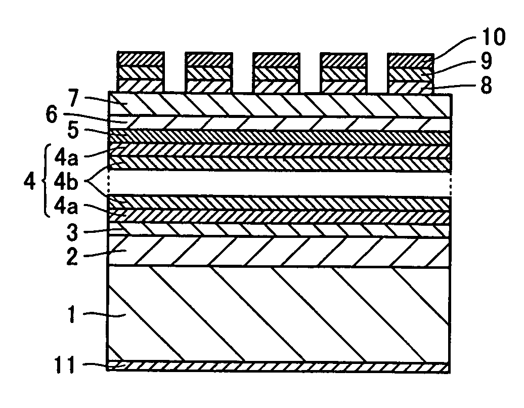
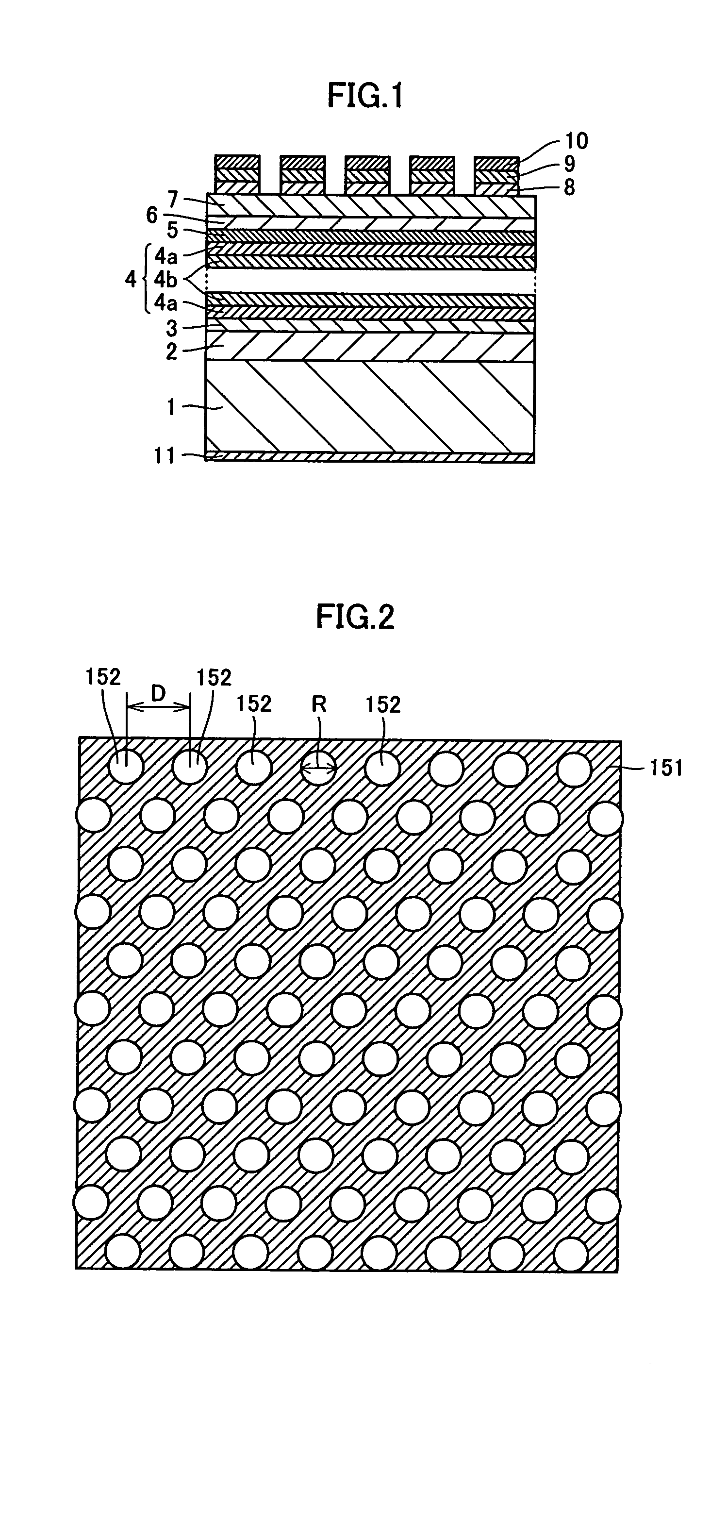
The structure of a nitride-based semiconductor LED according to a first embodiment of the present invention extracting light through a periodically formed electrode is described with reference to FIGS. 1 to 3.

In the nitride-based semiconductor LED according to the first embodiment, an n-type layer 2 of single-crystalline Si-doped GaN having a thickness of about 5 μm is formed on the (0001) Ga plane of an n-type GaN substrate 1 doped with oxygen or Si, as shown in FIG. 1. An n-type cladding layer 3 of single-crystalline Si-doped Al0.1Ga0.9N having a thickness of about 0.15 μm is formed on the n-type layer 2. A multiple quantum well (MQW) emission layer 4 having an MQW structure prepared by alternately forming six barrier layers 4a of single-crystalline undoped GaN each having a thickness of about 5 nm and five well layers 4b of single-crystalline undoped Ga0.9In0.1N each having a thickness of about 5 nm is formed on the n-type cladding layer 3. The MQW emission l...

second embodiment

(Second Embodiment)

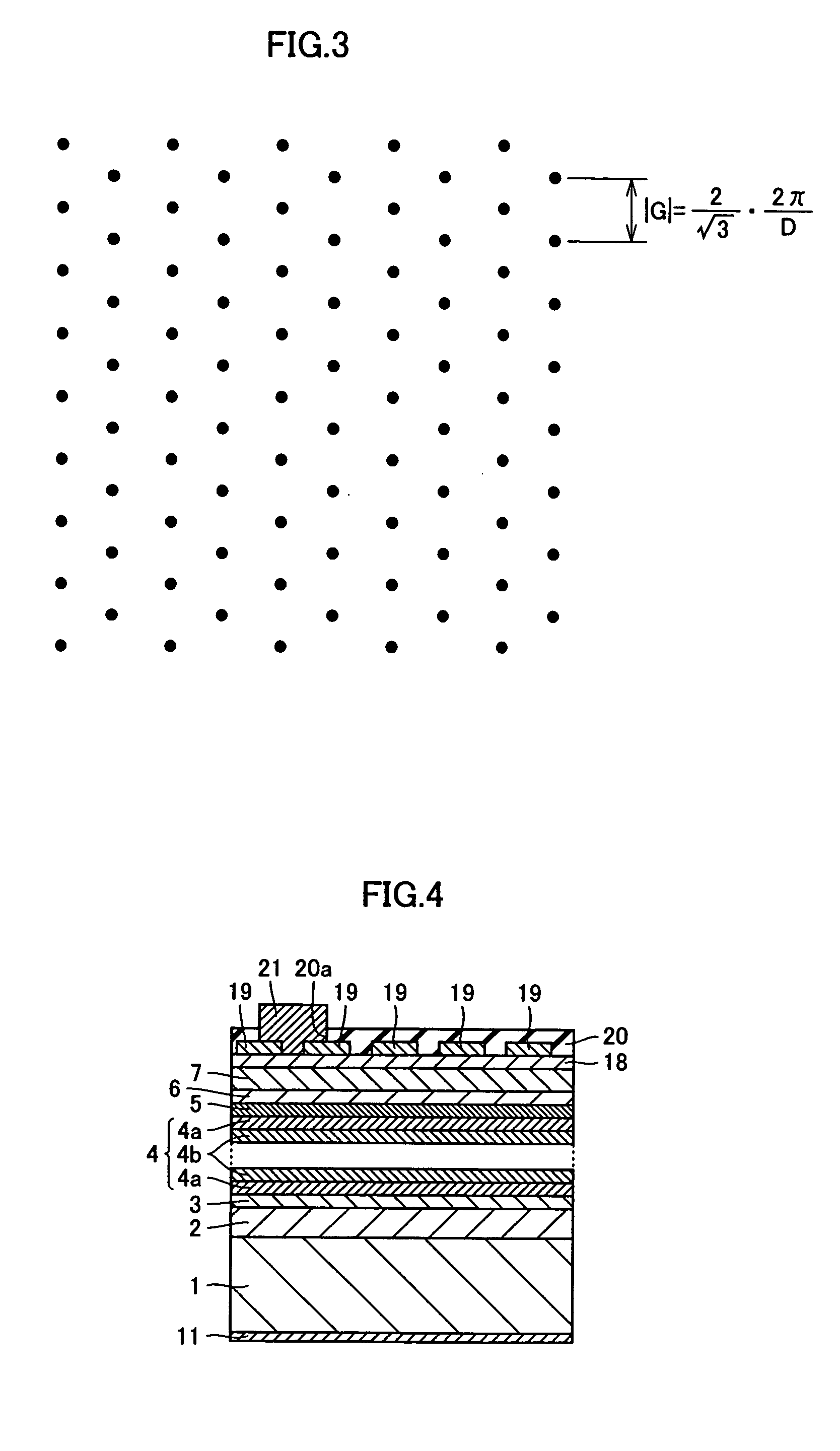
Referring to FIG. 4, a nitride-based semiconductor LED according to a second embodiment of the present invention is so formed that only an electrode 19 of a metal exhibiting a high plasma frequency has a periodic structure for extracting light through the electrode 19 having the periodic structure, dissimilarly to the aforementioned first embodiment.

According to the second embodiment, an ohmic electrode 18 of Pt having a thickness of about 1 nm is formed on the overall surface of a p-type contact layer 7, as shown in FIG. 4. The electrode 19, having a thickness of about 3 nm, of Al exhibiting a high plasma frequency is formed on the ohmic electrode 18 to have the periodic structure in the form of a triangular lattice similarly to that in the first embodiment shown in FIG. 2. The ohmic electrode 18 of Pt is superior to the electrode 19 of Al in ohmic property with respect to the p-type contact layer 7 of Mg-doped Ga0.95In0.05N. The electrode 19 consists of the m...

third embodiment

(Third Embodiment)

Referring to FIG. 5, a nitride-based semiconductor LED according to a third embodiment of the present invention is provided with a p-type contact layer 37 having a periodic corrugated shape on its surface, for extracting light from the side formed with the corrugated shape.

In the nitride-based semiconductor LED according to the third embodiment, circular portions (cylindrical projection or recess portions) 152 in the form of a (two-dimensional) triangular lattice corresponding to those shown in FIG. 2 are periodically formed on the surface of the p-type contact layer 37 of Mg-doped Ga0.95In0.05N. In this case, the distance D between each pair of adjacent circular portions (cylindrical projection or recess portions) 152 is set to 660 nm, and the diameter R of each circular portion (cylindrical projection or recess portion) 152 is set to 330 nm. The nitride-based semiconductor LED is designed on the assumption that the wavelength of light emitted from an emission ...


PUM


Abstract

A semiconductor light-emitting device capable of attaining a surface plasmon effect while attaining excellent ohmic contact is provided. This semiconductor light-emitting device comprises a semiconductor layer formed on an emission layer, a first electrode layer formed on the semiconductor layer and a second electrode layer, formed on the first electrode layer, having a periodic structure. The first electrode layer is superior to the second electrode layer in ohmic contact with respect to the semiconductor layer, and the second electrode layer contains a metal exhibiting a higher plasma frequency than the first electrode layer.

Description

BACKGROUND OF THE INVENTION 1. Field of the Invention The present invention relates to a semiconductor light-emitting device, and more particularly, it relates to a semiconductor light-emitting device including an electrode layer exhibiting a high plasma frequency. 2. Description of the Background Art In general, it is known as possible to excite surface plasmon (electronic oscillation) in a semiconductor light-emitting device by forming a metal layer exhibiting a high plasma frequency in a periodic structure, as disclosed in “Coupling of InGaN quantum-well photoluminescence to silver surface plasmons”, Phys. Rev. B60, 11564-11567, 15 October 1999, for example. It is possible to improve emission efficiency and light extraction efficiency by effectively utilizing the surface plasmon (electronic oscillation). Assuming that real parts of the dielectric constants εA and εB of a metal A and a dielectric B (including air or vacuum) have inverse signs, a light wave (electromagnetic wa...

Claims


Application Information

Patent Timeline
IPC IPC(8): H01L21/28G02B6/122H01L27/15H01L33/38H01L33/40H01S5/00H01S5/042H01S5/10H01S5/183H01S5/22H01S5/343
CPCB82Y20/00G02B6/1225G02B6/1226H01L33/387H01L33/405H01S2304/04H01S5/0425H01S5/1046H01S5/18319H01S5/34333H01L2933/0083H01S5/04252H01S5/04254
Inventor HATA, MASAYUKI
Owner EPISTAR CORP
Why Eureka
Try Eureka