

Pattern formation method
a pattern and pattern technology, applied in the field of pattern formation methods, can solve the problem that the amount of acid remaining on the resist pattern after the development is not sufficient for the crosslinking reaction, and achieve the effects of improving the reaction probability of the crosslinking reaction, low molecular weight, and high degree of movement freedom
- Summary
- Abstract
- Description
- Claims
- Application Information
AI Technical Summary
Benefits of technology
Problems solved by technology
Method used
Image

Examples
embodiment 1
[0034] A pattern formation method according to Embodiment 1 of the invention will now be described with reference to FIGS. 1A through 1D and 2A through 2C.
[0035] First, a positive chemically amplified resist material having the following composition is prepared:
Base polymer:poly(2-methyl-2-adamantyl acrylate-γ-2gbutyrolactone methacrylate)Acid generator:triphenylsulfonium nonaflate0.06gQuencher:triethanolamine0.002gSolvent:propylene glycol monomethyl ether acetate20g
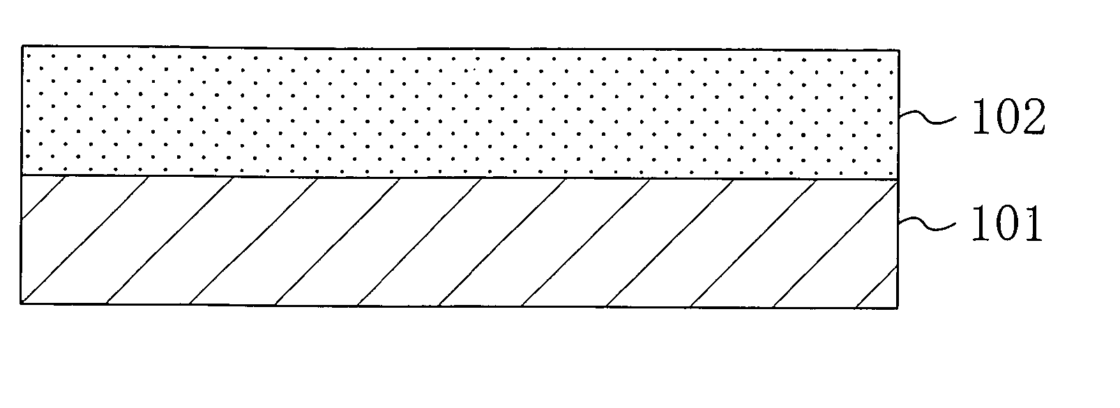
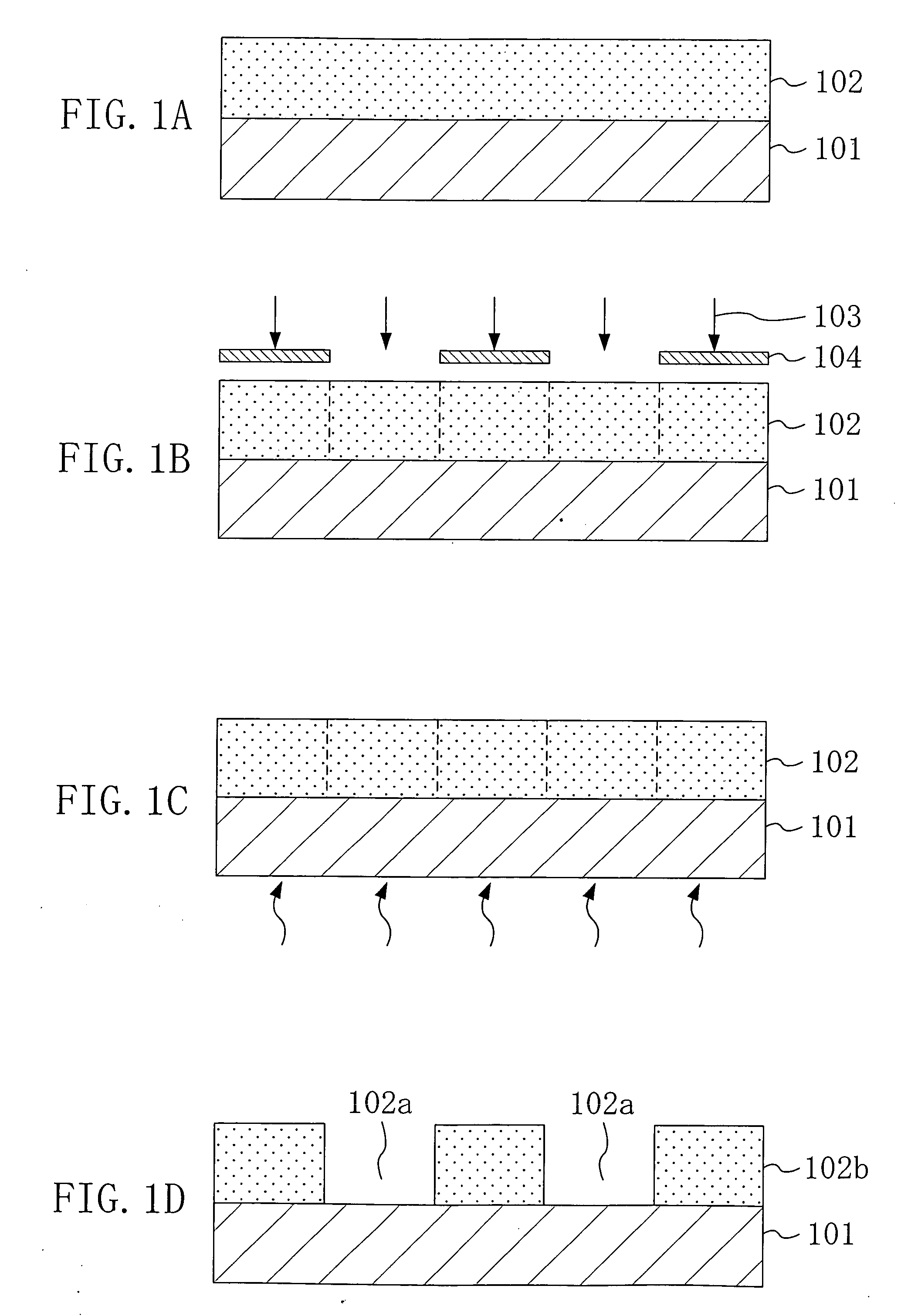
[0036] Next, as shown in FIG. 1A, the chemically amplified resist material is applied on a substrate 101, so as to form a resist film 102 with a thickness of 0.4 μm.
[0037] Then, as shown in FIG. 1B, the resist film 102 is subjected to pattern exposure by irradiating with exposing light 103 by using an ArF excimer laser scanner having numerical aperture (NA) of 0.60 through a mask 104.
[0038] After the pattern exposure, as shown in FIG. 1C, the resist film 102 is subjected to post-exposure bake (PEB) by using, for exa...
embodiment 2
[0047] A pattern formation method according to Embodiment 2 of the invention will now be described with reference to FIGS. 3A through 3D and 4A through 4C.
[0048] First, a positive chemically amplified resist material having the following composition is prepared:
Base polymer:poly(2-methyl-2-adamantyl acrylate-γ-2gbutyrolactone methacrylate)Acid generator:triphenylsulfonium nonaflate0.06gQuencher:triethanolamine0.002gSolvent:propylene glycol monomethyl ether acetate20g
[0049] Next, as shown in FIG. 3A, the chemically amplified resist material is applied on a substrate 201, so as to form a resist film 202 with a thickness of 0.4 μm.
[0050] Then, as shown in FIG. 3B, the resist film 202 is subjected to the pattern exposure by irradiating with exposing light 203 by using an ArF excimer laser scanner having numerical aperture (NA) of 0.60 through a mask 204.
[0051] After the pattern exposure, as shown in FIG. 3C, the resist film 202 is subjected to the post-exposure bake (PEB) by using,...
embodiment 3
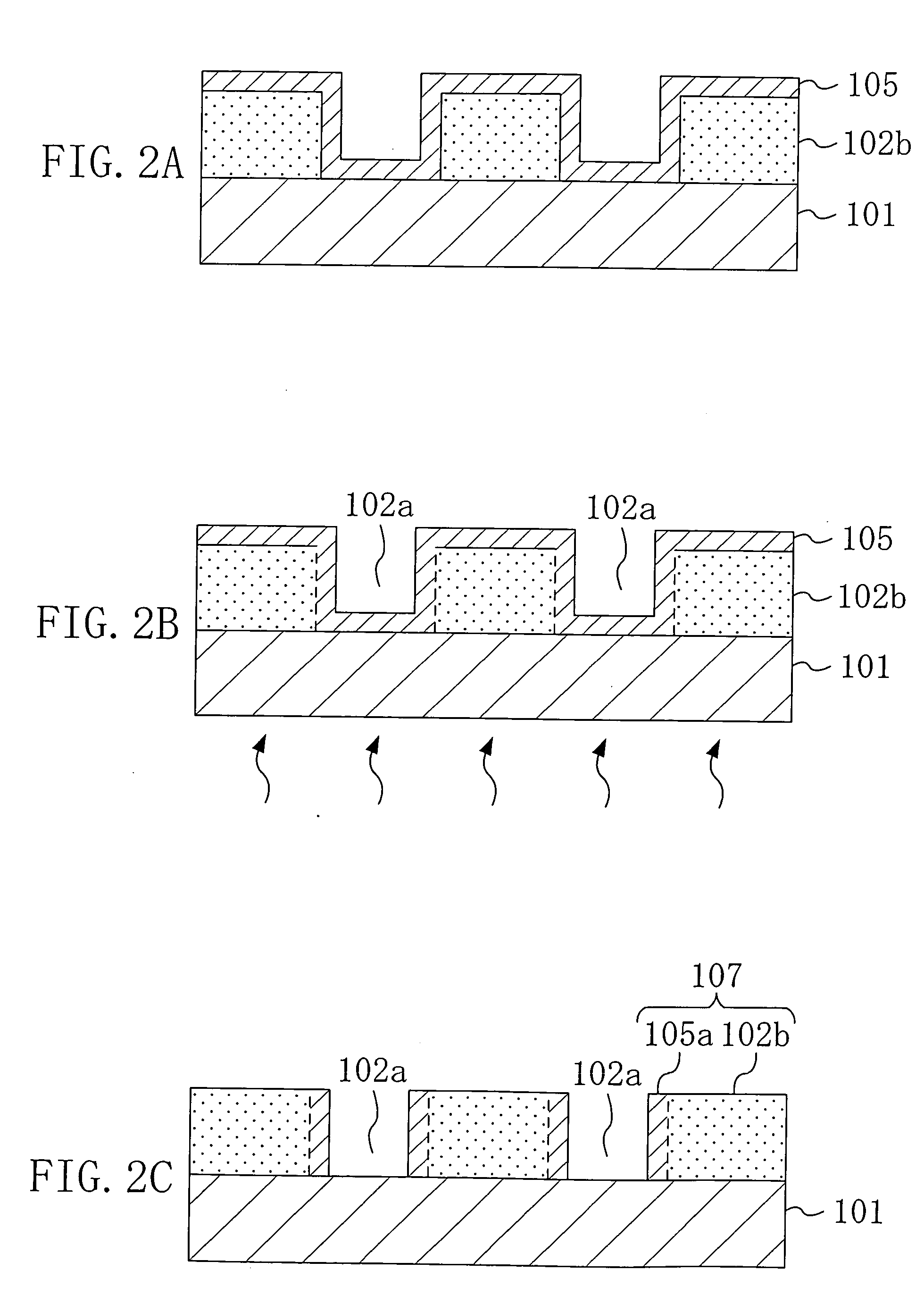
[0060] A pattern formation method according to Embodiment 3 of the invention will now be described with reference to FIGS. 5A through 5D and 6A through 6C.
[0061] First, a positive chemically amplified resist material having the following composition is prepared:
Base polymer:poly(2-methyl-2-adamantyl acrylate-γ-2gbutyrolactone methacrylate)Acid generator:triphenylsulfonium nonaflate0.06gQuencher:triethanolamine0.002gSolvent:propylene glycol monomethyl ether acetate20g
[0062] Next, as shown in FIG. 5A, the chemically amplified resist material is applied on a substrate 301, so as to form a resist film 302 with a thickness of 0.4 μm.
[0063] Then, as shown in FIG. 5B, the resist film 302 is subjected to the pattern exposure by irradiating with exposing light 303 by using an ArF excimer laser scanner having numerical aperture (NA) of 0.60 through a mask 304.
[0064] After the pattern exposure, as shown in FIG. 5C, the resist film 302 is subjected to the post-exposure bake (PEB) by using...
PUM
| Property | Measurement | Unit |
|---|---|---|
| diameter | aaaaa | aaaaa |
| diameter | aaaaa | aaaaa |
| thickness | aaaaa | aaaaa |
Abstract
Description
Claims
Application Information