Silicon-on-insulator wafer transfer method using surface activation plasma immersion ion implantation for wafer-to-wafer adhesion enhancement

a technology of surface activation and plasma immersion, which is applied in the direction of vacuum evaporation coating, transistors, coatings, etc., can solve the problems of insufficiently meeting the need for higher device speed and power consumption, prone to failure, and less useful structures

Inactive Publication Date: 2005-03-31
APPLIED MATERIALS INC
View PDF99 Cites 57 Cited by
  • Summary
  • Abstract
  • Description
  • Claims
  • Application Information

AI Technical Summary

Benefits of technology

[0011] A method of fabricating a semiconductor-on-insulator structure from a pair of semiconductor wafers, includes forming an oxide layer on at least a first surface of a first one of the wafers The method further includes performing a cleavage ion implantation step on one of the pair of wafers by ion implanting a specie to define a cleavage plane across a diameter of the wafer at the predetermined depth below the top surface of the one wafer and performing a bonding enhancement implantation step by ion implantation of a first species in the first surface of at least either o

Problems solved by technology

While such SOI structures provide the desired increase in device speed and/or decrease in power consumption, they are susceptible to failure by separation at the interface where the two wafers are conjoined.
This is because the silicon-to-silicon dioxide atomic bonds between the two wafers are or can be imperfect, in that they are not identical to (not as dense as) the ideal silicon-to-silicon dioxide bonds between a silicon wafer and the silicon dioxide layer formed on that wafer by a thermal process.
The problem of the tendency of SOI structures to failure by separation has thus far rendered SOI structures less useful than had been anticipated, so that the need for higher device speed and lower power consumption has not been fully met.
Another cause of the cleavage or separation problem is the susceptibility of the wafer-to-wafer bond to failure in the presence of contamination on the surface of either wafer prior to wafer-to-wafer bonding.
Thus, the SOI fabrication process is highly sensitive to contamination and is relatively unreliable as a result.
Another problem that must be addressed in SOI fabrication is the amending of the cleaved surface of the top ac

Method used


Image

  • Silicon-on-insulator wafer transfer method using surface activation plasma immersion ion implantation for wafer-to-wafer adhesion enhancement
  • Silicon-on-insulator wafer transfer method using surface activation plasma immersion ion implantation for wafer-to-wafer adhesion enhancement
  • Silicon-on-insulator wafer transfer method using surface activation plasma immersion ion implantation for wafer-to-wafer adhesion enhancement

Examples


Embodiment Construction

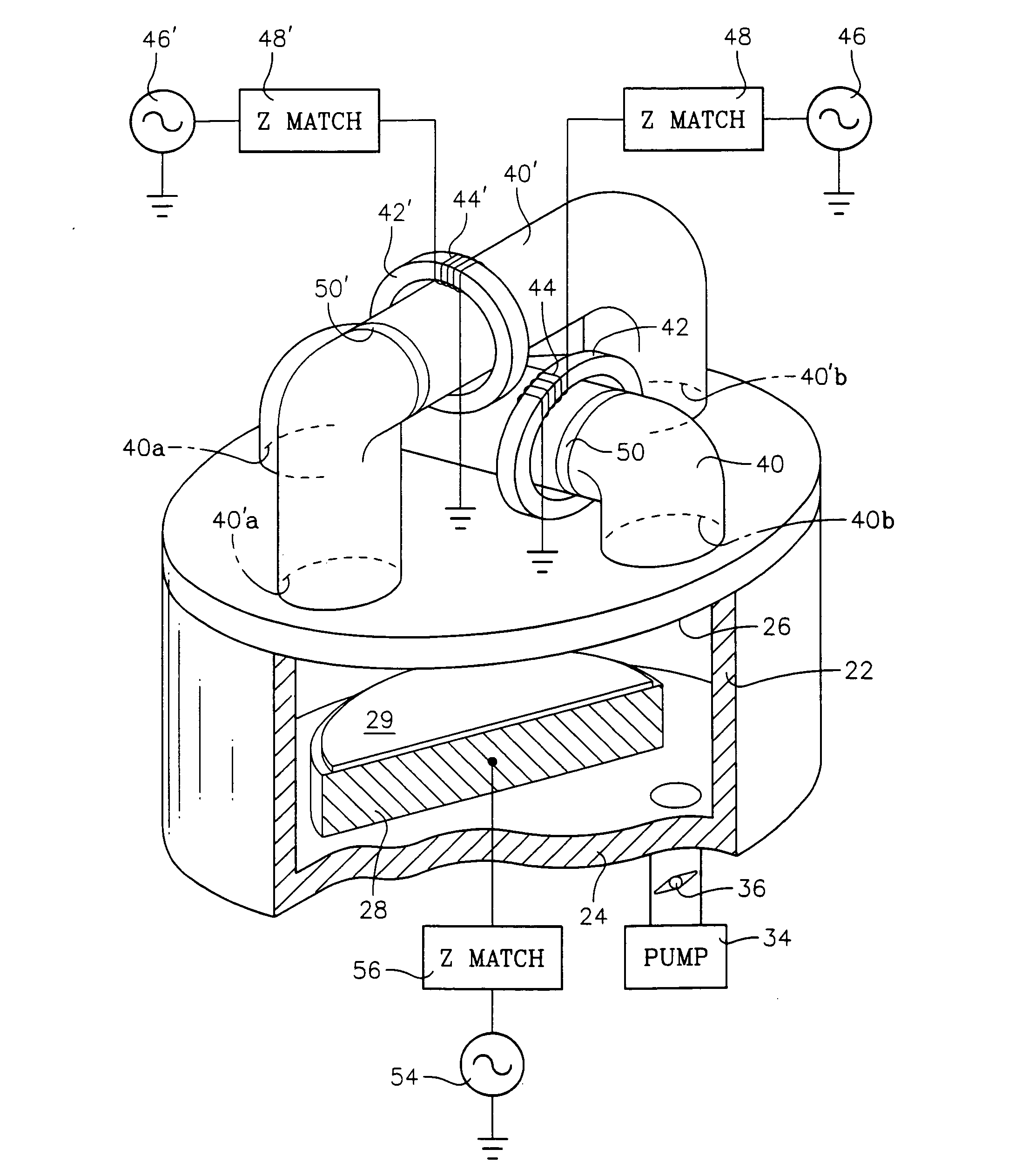
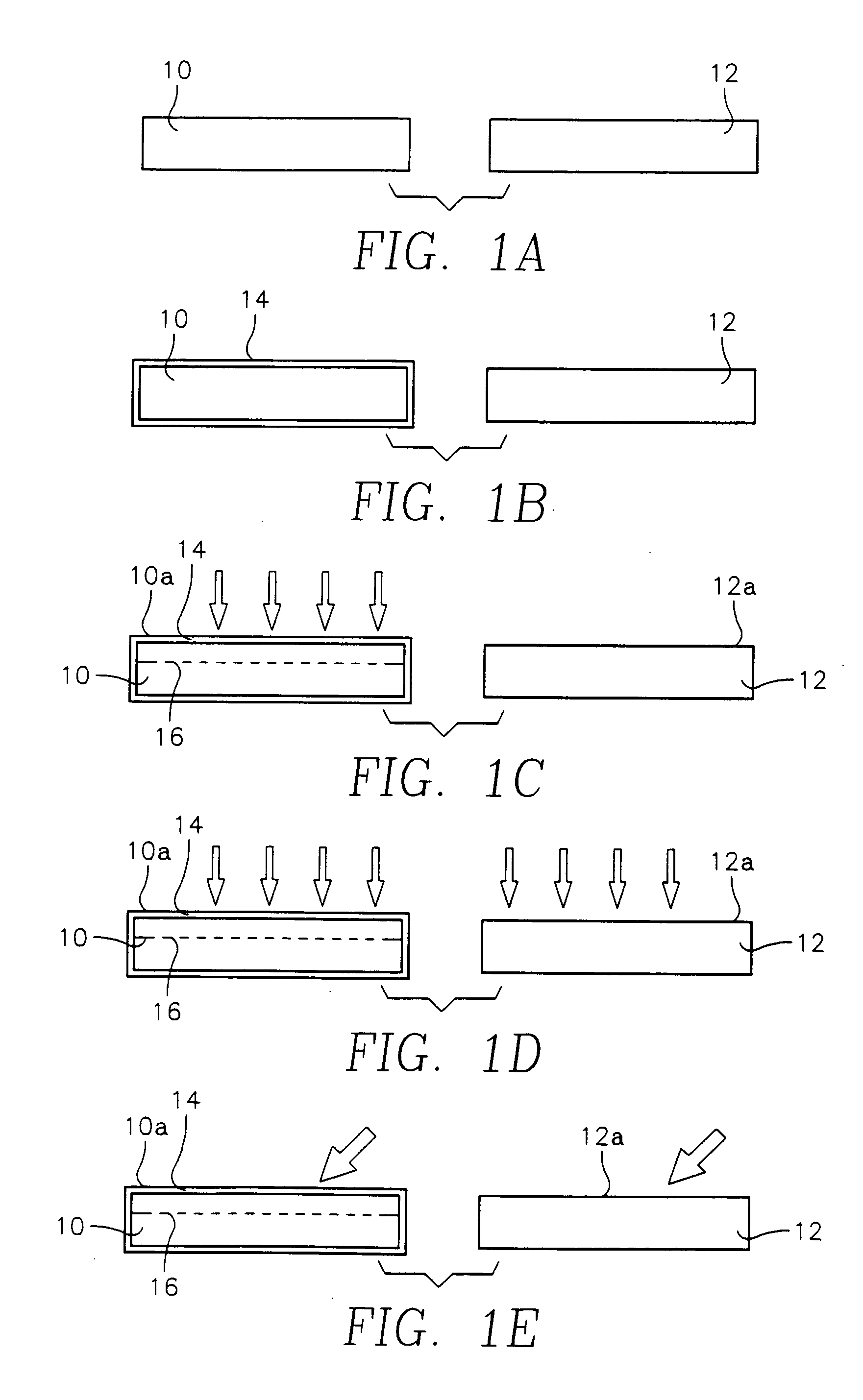
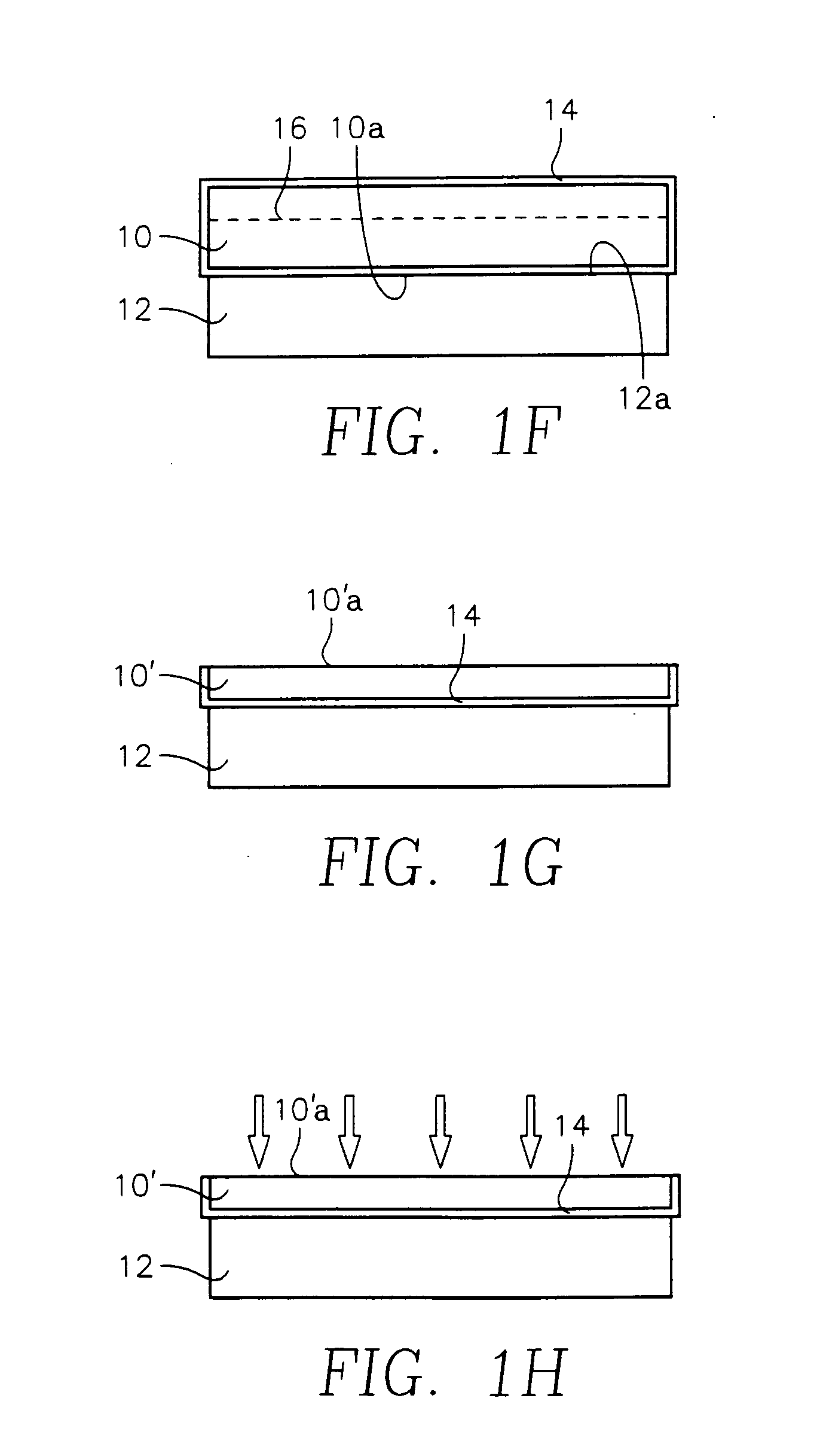
[0031]FIGS. 1A through 1H illustrate a sequence of steps in a wafer transfer SOI fabrication process in accordance with a first embodiment of the invention. FIGS. 2A and 2B illustrate the type of torroidal source plasma immersion ion implantation reactor that can be employed in carrying out some of the steps of the SOI fabrication process of FIGS. 1A through 1H. In FIG. 1A, a pair of wafers 10, 12 are provided. The wafers 10, 12 may be identical silicon crystalline wafers of the type employed in the manufacture of semiconductor microelectronic circuits. As one example, the wafers 10, 12 may be formed of intrinsic crystalline silicon and sliced to a thickness of about 2 mm from a cylindrical 300 mm diameter silicon boule along the silicon crystal 110 plane. Their surfaces may be polished to a micron smoothness. In the step of FIG. 1B, the wafer 10 is subjected to a thermal oxidation process to form a silicon dioxide film 14 on the top and back sides of the wafer 10. The thickness of ...


PUM

PropertyMeasurementUnit
Poweraaaaaaaaaa
Structureaaaaaaaaaa
Electric potential / voltageaaaaaaaaaa

Abstract

A method of fabricating a semiconductor-on-insulator structure from a pair of semiconductor wafers, includes forming an oxide layer on at least a first surface of a first one of the wafers and performing a bonding enhancement implantation step by ion implantation of a first species in the first surface of at least either of the pair of wafers. The method further includes performing a cleavage ion implantation step on one of the pair of wafers by ion implanting a second species to define a cleavage plane across a diameter of the wafer at the predetermined depth below the top surface of the one wafer. The wafers are then bonded together by placing the first surfaces of the pair of wafers onto one another so as to form an semiconductor-on-insulator structure. The method also includes separating the one wafer along the cleavage plane so as to remove a portion of the one wafer between the second surface and the cleavage plane, whereby to form an exposed cleaved surface of a remaining portion of the one wafer on the semiconductor-on-insulator structure. Finally, the cleaved surface is smoothed, preferably by carrying out a low energy high momentum ion implantation step.

Description

CROSS-REFERENCE TO RELATED APPLICATIONS [0001] This application is a continuation-in-part of U.S. application Ser. No. 10 / 838,052 filed May 3, 2004 entitled VERY LOW TEMPERATURE CVD PROCESS WITH CONFORMALITY, STRESS AND COMPOSITION OF THE CVD LAYER by Hiroji Hanawa, et al. (the disclosure of which is incorporated herein by reference), which is a continuation-in-part of U.S. application Ser. No. 10 / 786,410 filed Feb. 24, 2004 entitled FABRICATION OF SILICON-ON-INSULATOR STRUCTURE USING PLASMA IMMERSION ION IMPLANTATION by Daniel Maydan, et al., which is a continuation-in-part of U.S. application Ser. No. 10 / 646,533 filed Aug. 22, 2003 entitled PLASMA IMMERSION ION IMPLANTATION PROCESS USING A PLASMA SOURCE HAVING LOW DISSOCIATION AND LOW MINIMUM PLASMA VOLTAGE by Kenneth Collins, et al., which is a continuation-in-part of U.S. application Ser. No. 10 / 164,327 filed Jun. 5, 2003 entitled EXTERNALLY EXCITED TORROIDAL PLASMA SOURCE WITH MAGNETIC CONTROL OF ION DISTRIBUTION by Kenneth Col...

Claims


Application Information

Patent Timeline
IPC IPC(8): H01J37/32
CPCC23C14/48H01L29/6659H01J37/32082H01J37/321H01J37/32357H01J37/32412H01L21/2236H01L21/26513H01L21/31604H01L21/318H01L21/76254H01L21/823807H01L21/823814H01L21/823842C23C16/507
Inventor AL-BAYATI, AMIRCOLLINS, KENNETH S.HANAWA, HIROJIRAMASWAMY, KARTIKGALLO, BIAGIONGUYEN, ANDREW
Owner APPLIED MATERIALS INC
Why Eureka
Try Eureka