Multi-layered complementary wire structure and manufacturing method thereof

a manufacturing method and complementary wire technology, applied in the direction of identification means, instruments, semiconductor devices, etc., can solve the problems of limiting the design and manufacture of the device, affecting reducing so as to increase the operating speed of the device, reduce the resistance of the overall wire, and increase the open ratio of the pixel unit

Inactive Publication Date: 2005-04-07
IND TECH RES INST
View PDF2 Cites 26 Cited by
  • Summary
  • Abstract
  • Description
  • Claims
  • Application Information

AI Technical Summary

Benefits of technology

With the application of a multi-layered complementary wire structure and a manufacturing method thereof of the present invention, the resistance of the overall wire can be reduced to increase the operating speed of the device, and the open ratio of the pixel unit can be increased as well.

Problems solved by technology

A conventional display composed of a cathode ray tube (CRT) or image tube is too large to satisfy the current demands for compact, lightweight equipment.
At present, displays are becoming larger and the lengths of the gate lines and the data lines are becoming longer, and thus the overall resistance is increasing to cause serious resistance capacitance delay (RC Delay), thereby limiting the design and manufacture of the device and affecting the operating speed of the device.

Method used


Image

  • Multi-layered complementary wire structure and manufacturing method thereof
  • Multi-layered complementary wire structure and manufacturing method thereof
  • Multi-layered complementary wire structure and manufacturing method thereof

Examples


Embodiment Construction

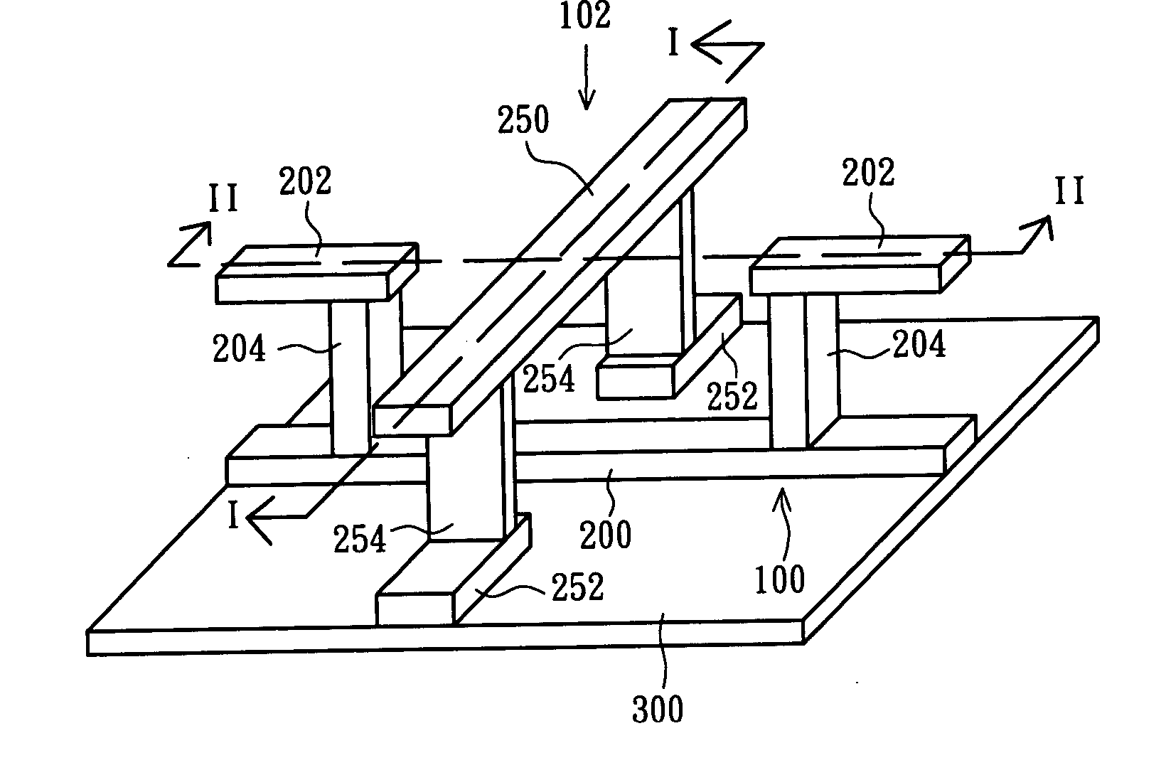
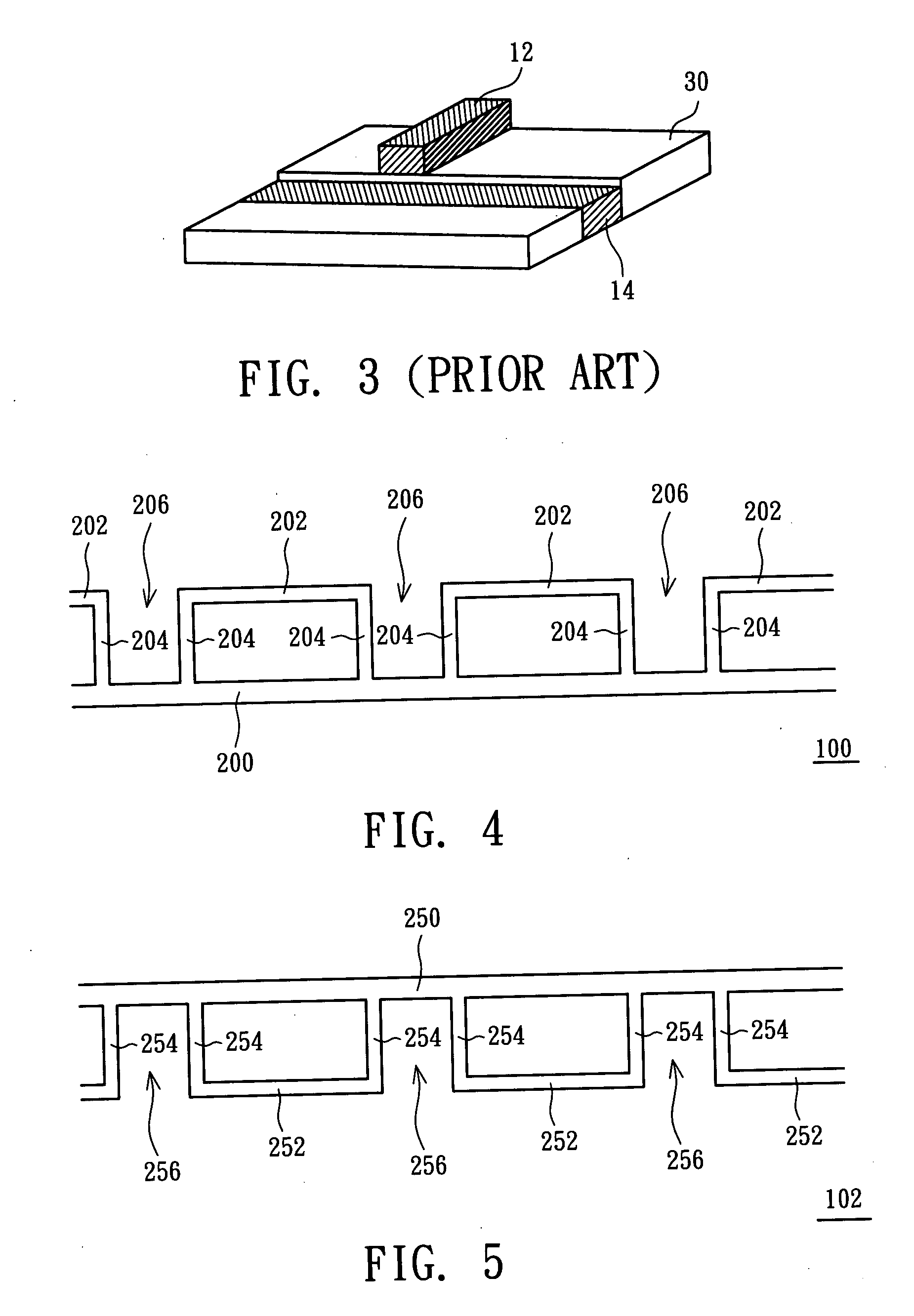
The present invention discloses a wire structure having a multi-layered complementary feature. The following is an illustration in accordance with a preferred embodiment of the present invention. In order to make the illustration of the present invention more explicit and complete, the following description and the drawings from FIG. 4 to FIG. 9 are provided.

FIG. 4 illustrates a cross-sectional view of a wire structure of a gate line in accordance with a preferred embodiment of the present invention. Referring to FIG. 4, a wire structure 100 used as a gate line in a display of the present invention comprises a slender main line 200 and a plurality of branch lines 202 located in-line and separated. Because the main line 200 and the branch lines 202 are located in different layers, two ends of each of the branch lines 202 are connected to the main line 200 by plugs 204, thus forming a double-layered, toothlike wire structure comprising a plurality of fillisters 206.

A formula for c...


PUM

PropertyMeasurementUnit
structureaaaaaaaaaa
conductiveaaaaaaaaaa
matrix structureaaaaaaaaaa

Abstract

A multi-layered complementary wire structure and a manufacturing method thereof are disclosed, comprising a first wire and a second wire. Each of the first and the second wires comprises a main line and a plurality of branch lines located in a different layer from the main line. A plurality contact holes are formed in an insulating layer between the first wire and the second wire to connect the main line of the first wire and the branch lines of the first wire, and connect the main line of the second wire and the branch lines of the second wire. The main line of the first wire is insulated and crossed with the main line of the second wire. The main line of the first wire and the branch lines of the second wire are insulated with each other and located in the same layer. The main line of the second wire and the branch lines of the first wire are insulated with each other and located in the same layer.

Description

FIELD OF THE INVENTION The present invention relates to a multi-layered complementary wire structure and a manufacturing method thereof, and more particularly, to a multi-layered complementary wire structure and a manufacturing method thereof that can substantially reduce the resistance of the wire. BACKGROUND OF THE INVENTION With the rapid development of multimedia, user requirements for peripheral audio-visual equipment are raised accordingly. A conventional display composed of a cathode ray tube (CRT) or image tube is too large to satisfy the current demands for compact, lightweight equipment. Recently, many flat panel display technologies, such as liquid crystal display (LCD), plasma display panel (PDP) display and field emission display (FED), have been developed sequentially and have become the mainstream for future display. FIG. 1 illustrates a schematic diagram of a thin film transistor array plate of a conventional display. Referring to FIG. 1, a thin film transistor arr...

Claims


Application Information

Patent Timeline
Patent Type & Authority Applications(United States)
IPC IPC(8): G02F1/1362G09F9/30H01L23/522H01L27/12
CPCG02F1/136286H01L23/5221H01L27/12H01L2924/0002H01L2924/00
Inventor CHEN, YU-CHENGCHEN, CHI-LIN
Owner IND TECH RES INST
Why Eureka
Try Eureka