Optical recording medium
a recording medium and optical technology, applied in the field of optical recording mediums, can solve the problems of serious storage stability and deterioration of the storage stability of the recording medium, and achieve the effects of satisfying the recording characteristics and storage stability, rewriting cyclability and storage stability, and high density recording
- Summary
- Abstract
- Description
- Claims
- Application Information
AI Technical Summary
Benefits of technology
Problems solved by technology
Method used
Image
Examples
example 1
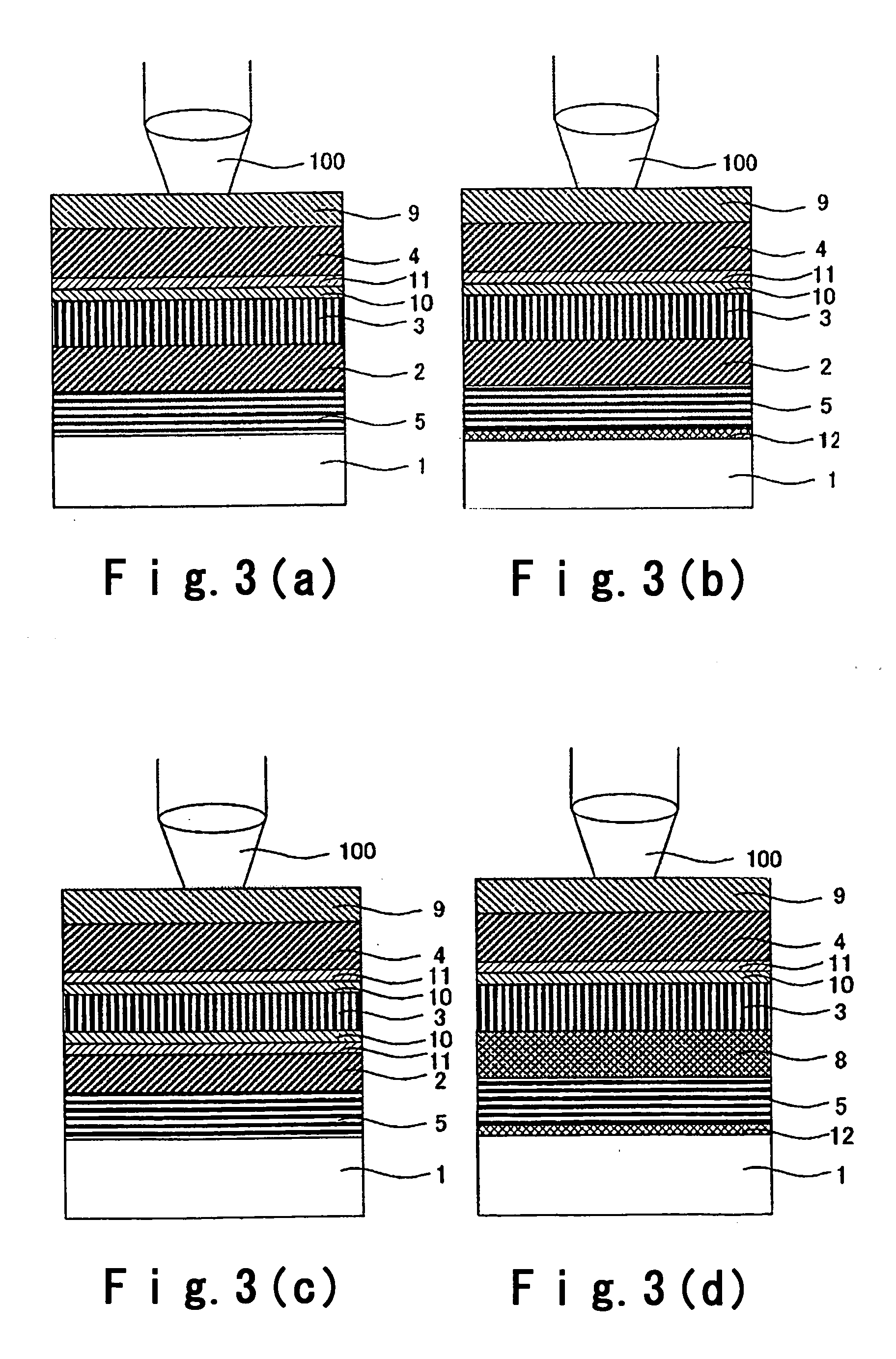
[0205] As an embodiment of the present invention, an optical recording medium having a structure shown in FIG. 3(d) was prepared.
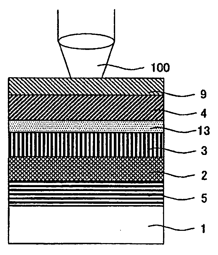
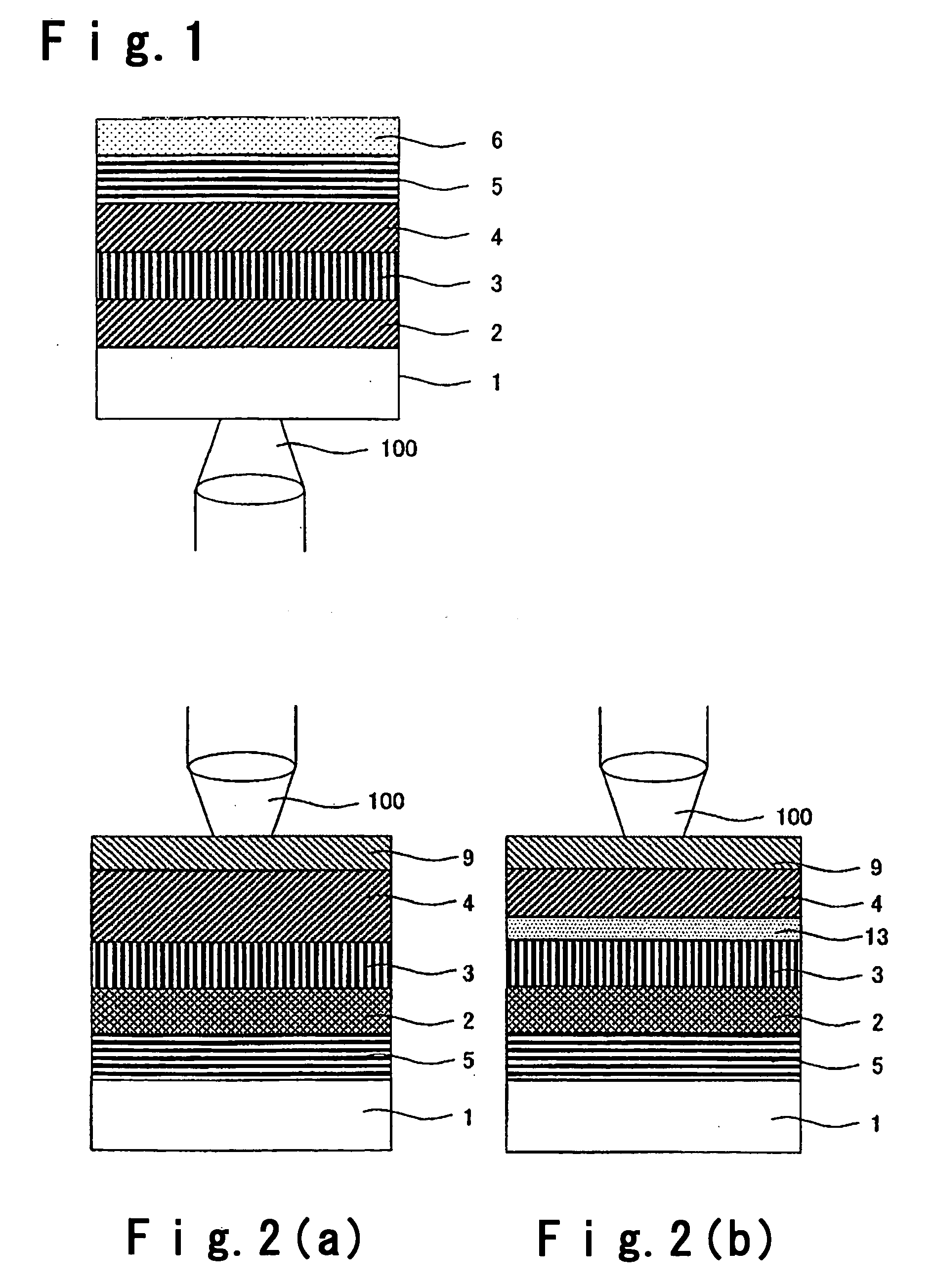
[0206] As the substrate 1, a disk shaped polycarbonate resin having a thickness of 1.1 mm and a diameter of 120 mm was employed. For the protective layer 4, a mixture comprising ZnS—SiO2 was employed. For the recording layer 3, an alloy comprising In—Ge—Sb—Te was employed. For the reflective layer 5, an alloy comprising Ag—Cu—Au was employed. For the interface layer 8 as a substitute for the protective layer and for the under layer 12, GeCrN was employed, and further for the first diffusion preventing layer 10 and for the second diffusion preventing layer 11, GeCrN (one having the concentration of the N component changed) was employed.
[0207] With respect to the light transmitting layer 9, 2.5 g of an uncured (non-polymerized) acrylate type ultraviolet curable agent having a viscosity of 3000 mPa·s was dropped in the vicinity of the center of the protecti...
example 2
[0267] Then, the following disks 10 to 13 were prepared to make clear the effects of the thickness of the protective-layer on the incident side and of the presence or absence of the under layer in the film side incident type optical recording medium.
[0268] As disk 10, an optical recording medium of a structure having the under layer 12 removed from FIG. 3(d), was prepared. The substrate 1 and the light transmitting layer 9 were exactly the same as in Example 1. Also with respect to the protective layer 4, the reflective layer 5, the interface layer 8 as a substitute for the protective layer, the recording layer 3, the first diffusion preventing layer 10 and the second diffusion preventing layer 11, the same materials as in Example 1 were employed, and they were prepared by a sputtering method. The film forming conditions and the film thicknesses of the respective layers are as follows.
[0269] (B) Metal Reflective Layer 5[0270] Sputtering target: Ag97Cu1Au2 (atomic %) [0271] Sputter...
PUM
| Property | Measurement | Unit |
|---|---|---|
| thickness | aaaaa | aaaaa |
| thickness | aaaaa | aaaaa |
| diameter | aaaaa | aaaaa |
Abstract
Description
Claims
Application Information


