Fully dry, Si recess free process for removing high k dielectric layer
a dielectric layer, fully dry technology, applied in the direction of crystal growth process, polycrystalline material growth, chemically reactive gas growth, etc., can solve the problems of low selectiveness of hf, inability to easily form volatile by-products, and inability to give detailed details of the etch process. cost
- Summary
- Abstract
- Description
- Claims
- Application Information
AI Technical Summary
Benefits of technology
Problems solved by technology
Method used
Image

Examples
Embodiment Construction
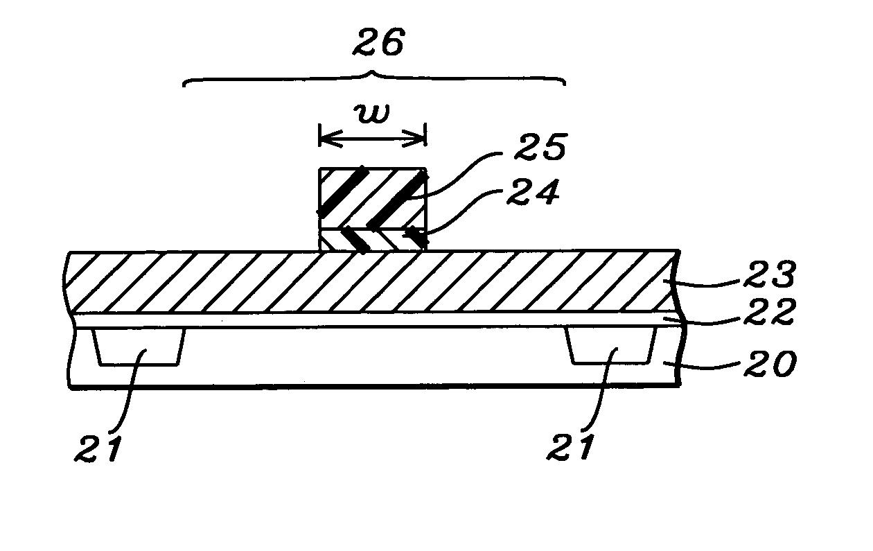
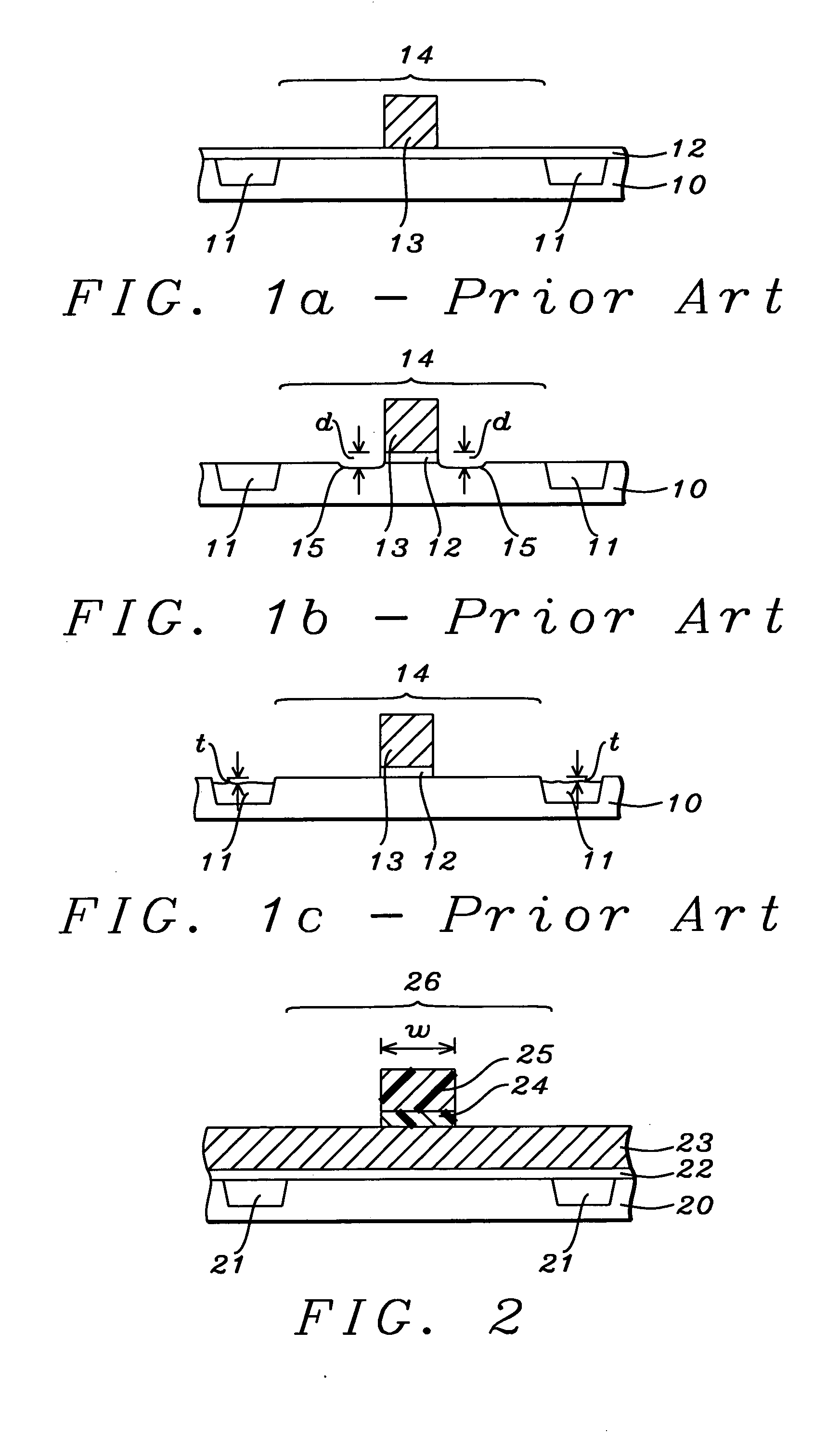
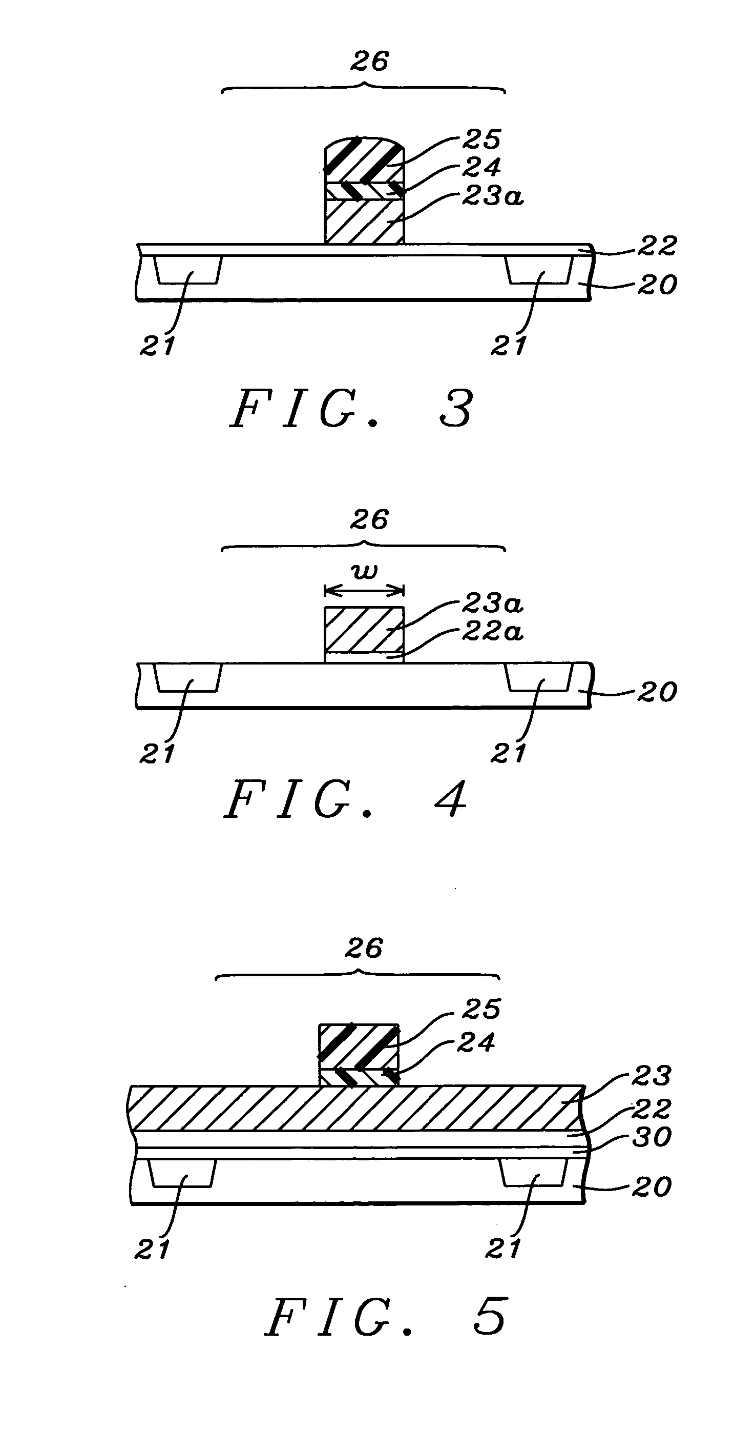
[0023] The present invention is a method of removing a high k dielectric layer from a substrate. Although a description is provided with regard to a high k gate dielectric layer on a substrate in a partially formed metal oxide semiconductor field effect transistor (MOSFET) which may be a p-type (PMOS) or n-type (NMOS) transistor, the substrate with a high k dielectric layer formed thereon may be used to fabricate other semiconductor devices including capacitors. The drawings are not intended to limit the scope of the invention and the figures are not necessarily drawn to scale.
[0024] Referring to FIGS. 1a-1c, a method of etching a high k dielectric layer that has been previously practiced by the inventors is illustrated. In FIG. 1a, a substrate 10 is provided that has shallow trench isolation (STI) features 11 which define an active region 14. A high k dielectric layer 12 that is HfO2 is deposited on substrate 10 and a gate electrode 13 is formed by a conventional method that invol...
PUM
 Abstract
Description
Claims
Application Information
 - Generate Ideas
- Intellectual Property
- Life Sciences
- Materials
- Tech Scout
- Unparalleled Data Quality
- Higher Quality Content
- 60% Fewer Hallucinations
Browse by: Latest US Patents, China's latest patents, Technical Efficacy Thesaurus, Application Domain, Technology Topic, Popular Technical Reports.
© 2025 PatSnap. All rights reserved.Legal|Privacy policy|Modern Slavery Act Transparency Statement|Sitemap|About US| Contact US: help@patsnap.com