Pasted soi substrate, process for producing the same and semiconductor device

a soi substrate and semiconductor technology, applied in the direction of semiconductor devices, electrical devices, transistors, etc., can solve the problems of difficult control of the dimension of the trench to be formed in the surface of the semiconductor substrate, and/or the heat treatment condition for forming the plate-like cavity through the migration of silicon atoms, and achieve the effect of optimal

Active Publication Date: 2005-04-21
SUMITOMO MITSUBISHI SILICON CORP
View PDF22 Cites 36 Cited by
  • Summary
  • Abstract
  • Description
  • Claims
  • Application Information

AI Technical Summary

Benefits of technology

[0052] When the channel of the unit transistor is formed in this region, such a semiconductor device of mixed loading type can be obtained, which allows the feature of each element to be functioned in an optimally effective manner respectively.

Problems solved by technology

However, according to the prior art semiconductor substrate and manufacturing method thereof, a control of the dimension of the trench to be formed in the surface of the semiconductor substrate and / or a control of the heat treatment condition for forming the plate-like cavity through the migration of the silicon atoms have been found difficult.
Consequently, it has been difficult to fabricate the SOI structure exactly as specified in its design.

Method used


Image

  • Pasted soi substrate, process for producing the same and semiconductor device
  • Pasted soi substrate, process for producing the same and semiconductor device
  • Pasted soi substrate, process for producing the same and semiconductor device

Examples


first embodiment

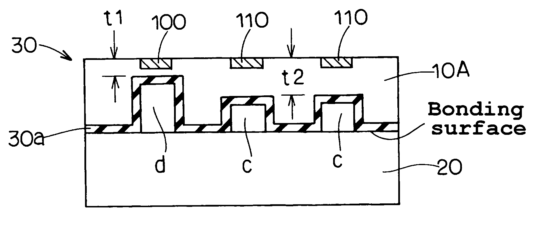
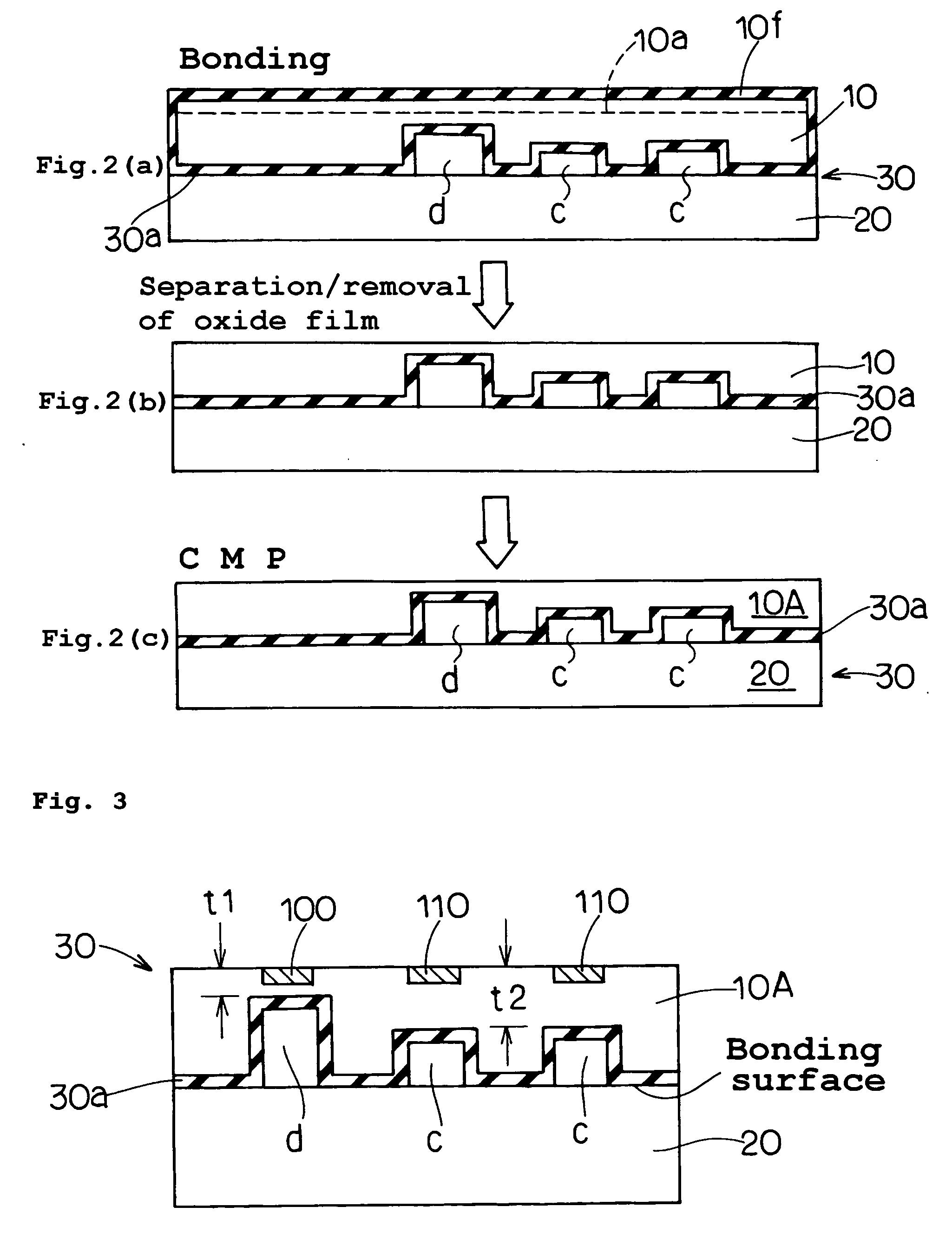
[0063] Referring to FIG. 1 through FIG. 3, a bonded SOI substrate and a manufacturing method thereof according to the present invention will be described.

[0064] The bonded SOI substrate according to this embodiment is characterized in that a predetermined number of shorter cavities “c” and a predetermined number of taller cavities “d” defining their heights taller than said shorter cavities “c” reside in an active layer wafer 10 side with respect to a bonding interface between an active layer 10A and a supporting substrate wafer 20. This difference in height results in a difference in thickness of the SOI layer (active layer) 10A in these regions. In FIG. 3, the SOI layer 10A having the thickness “t1” is formed above the cavity “d” and the SOI layer 10A having the thickness “t2” is formed above the cavity “c”, respectively. It is to be noted that t1

[0065] As it is, a CMOS transistor 100 will be formed in this region of the thinner silicon layer and a bipolar transistor 110 will...

second embodiment

[0079] Turning now to FIG. 4 through FIG. 6, the present invention is illustrated.

[0080] The manufacturing method of the SOI substrate according to this embodiment is characterized in that in the step prior to the hydrogen ion implantation, firstly a silicon-germanium thin film 10b is epitaxially-grown on the surface (mirror-surface) of the active layer silicon wafer 10, and secondly a silicon thin film 10c is successively epitaxially-grown on the surface of the silicon-germanium thin film 10b, as shown in FIG. 4.

[0081] It is to be noted that as the active layer silicon wafer 10, such a silicon wafer may be employed that has been pulled up by the CZ method (Czochralski method) and processed by the slicing, beveling, lapping, etching and mirror-surface polishing.

[0082] Subsequently, the hydrogen ions are implanted into the interface between this silicon-germanium (SiGe) thin film 10b and the active layer wafer 10 or into the SiGe film 10b, or otherwise into the silicon substrate im...

third embodiment

[0093] Referring now to FIG. 7 through FIG. 9, the present invention is illustrated.

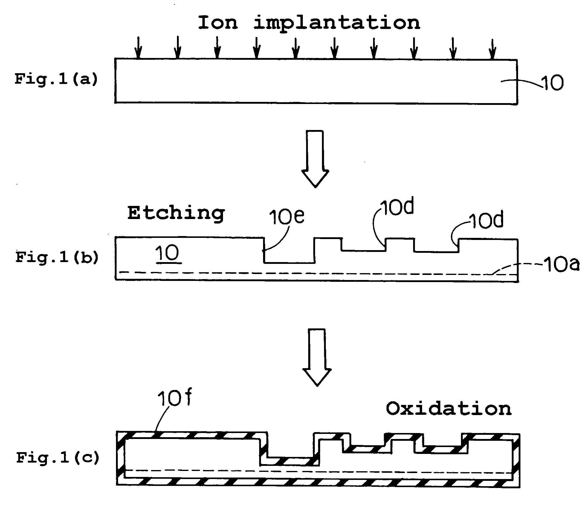
[0094] Firstly, a single crystal silicon ingot that has been pulled up by the CZ method is further processed through the slicing, beveling, lapping, etching and polishing to thereby prepare the active layer wafer 10 having a thickness of 725 μm, a diameter of 200 nm, and an initial oxygen concentration of 14.0×10¹⁷ atoms / cc, with its surface having been mirror-surface finished (FIG. 7).

[0095] Secondly, hydrogen ions are implanted at a rate of 5.0×10¹⁶ atoms / cm2 into the active layer wafer 10 by using a medium current ion implanter with an accelerating voltage of 100 keV so as to achieve the depth of implantation of about 2 μm from the wafer surface side. In this way, the hydrogen ion implanted layer 10a is formed in the surface layer of the active wafer 10 at a predetermined depth from a surface thereof as an extending plane.

[0096] On the other hand, the supporting substrate wafer 20 is prepared by...


PUM


Abstract

A plurality of recessed portions having different depths is formed in a surface of the active layer wafer or in a bonding surface of the supporting substrate wafer. Those wafers are bonded to each other with an insulation film interposed therebetween. This allows a cavity of higher dimensional precision to be buried therein. A plurality of cavities may be formed simultaneously in a plurality of locations within the plane of the substrate, which allows the thickness of the SOI layer to be set arbitrarily. Accordingly, such a semiconductor device can be fabricated easily in which a MOS type element and a bipolar element are formed on the same chip in a mixed manner.

Description

FIELD OF THE INVENTION [0001] The present invention relates to a bonded SOI substrate and a manufacturing method thereof and a semiconductor device using said substrate, and more specifically to a technology in which after an active layer wafer and a supporting substrate wafer having been bonded to each other with an insulation layer interposed between them, the active layer wafer is thinned to define a SOI layer. DESCRIPTION OF THE PRIOR ART [0002] In a trend of increasing demand for higher integration as well as more multi-functionality in a LSI fabricated on a silicon substrate, separation among respective elements turns out now to be a subject of importance. In the LSI according to the prior art, which typically resides on a silicon wafer having a thickness in a range of 500 μm to 800 μm, electronic circuit elements are integrally fabricated in a surface layer thereof (defined by a depth of some ten μm from a surface). [0003] A SOI (Silicon On Insulator) substrate has been known...

Claims


Application Information

Patent Timeline
Patent Type & Authority Applications(United States)
IPC IPC(8): H01L21/02H01L21/336H01L21/762H01L21/764H01L27/12H01L29/786
CPCH01L21/76251H01L21/764H01L21/76254H01L27/12
Inventor ADACHI, NAOSHINAKAMAE, MASAHIKO
Owner SUMITOMO MITSUBISHI SILICON CORP
Why Eureka
Try Eureka