Plasma processing equipment

Inactive Publication Date: 2005-04-21
TOKYO ELECTRON LTD
View PDF12 Cites 30 Cited by
  • Summary
  • Abstract
  • Description
  • Claims
  • Application Information

AI Technical Summary

Benefits of technology

[0028] As a result of this, since microwave can be propagated in the TEM mode from the microwave generating source, a

Problems solved by technology

Consequently, multiple reflections of microwave or the like occur in such discontinuities, inevitably resulting in heat production due to the Joule heat generated from line resistance.
Further, another problem exists as follows.
Accordingly, since the mode converter 32 is required, the cost of the plasma processing appara

Method used


Image

  • Plasma processing equipment
  • Plasma processing equipment
  • Plasma processing equipment

Examples


Embodiment Construction

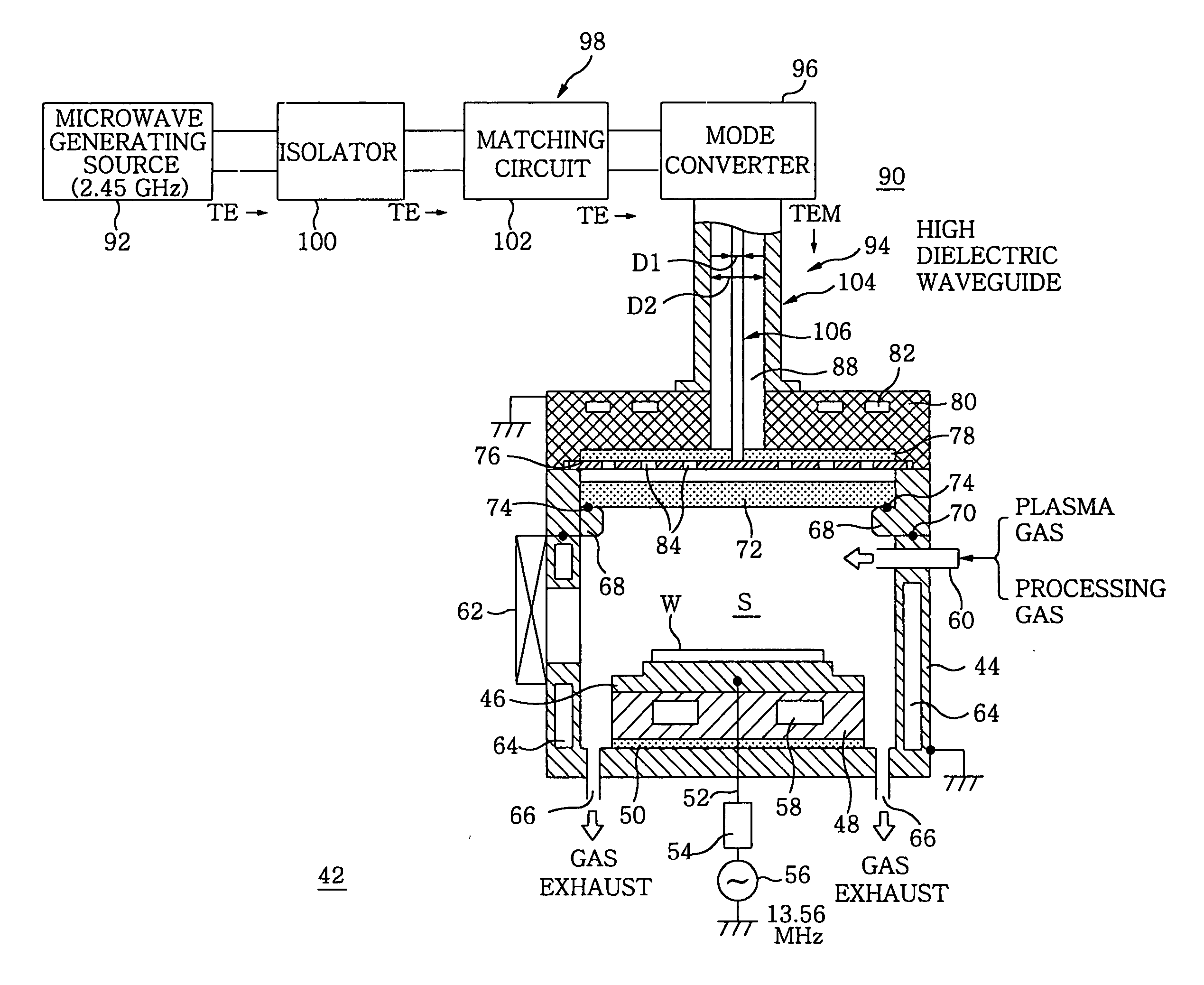
[0041] Hereinafter, a plasma processing apparatus in accordance with a first preferred embodiment of the present invention is described in detail with reference to the accompanying drawings.

[0042] First, a first preferred embodiment of the present invention is discussed.

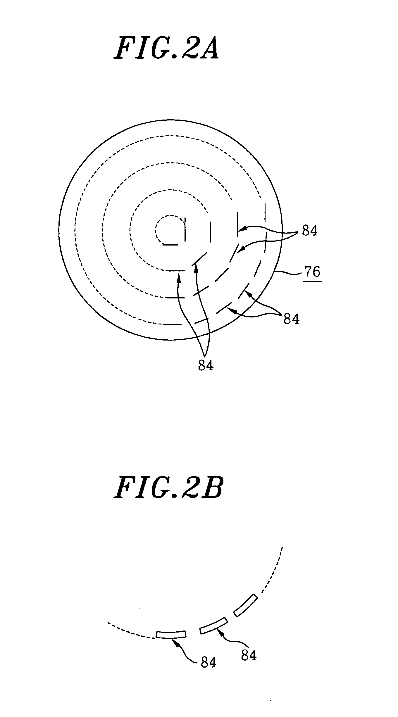
[0043]FIG. 1 illustrates the configuration of a plasma processing apparatus in accordance with the first embodiment and FIGS. 2A and 2B are a plan view illustrating an example of a flat antenna member employed in the apparatus. FIGS. 3A and 3B show a plan view of another example of the flat antenna member and FIG. 4 shows a simulation model of microwave transmission in a high dielectric waveguide used in the first embodiment. FIG. 6 illustrates a simulation model of microwave transmission in another type of high dielectric waveguide. In the present invention, a high dielectric material refers to a dielectric material having a relative dielectric constant higher than that of a typical dielectric material, for exampl...


PUM

PropertyMeasurementUnit
Angleaaaaaaaaaa
Dielectric polarization enthalpyaaaaaaaaaa
Dielectric constantaaaaaaaaaa

Abstract

Plasma processing equipment capable of increasing the heat resistance of a wave guide by using a high dielectric material, comprising a processing container 44 formed to allow vacuuming, a loading table 46 installed in the processing container for placing a processed body W thereon, a microwave transmission plate 72 installed in an opening part at the ceiling of the processing container, a flat antenna member 76 for feeding microwave into the processing container through the microwave transmission plate, a shield cover body 80 earthed so as to cover the upper part of the flat antenna member, and a waveguide 90 for feeding the microwave from a microwave generating source to the flat antenna member, characterized in that the waveguide is formed of a high dielectric waveguide 94 using the high dielectric material, whereby the heat resistance of the waveguide can be increased.

Description

FIELD OF THE INVENTION [0001] The present invention relates to a plasma processing apparatus for processing a semiconductor wafer or the like by subjecting it to a plasma produced by microwave. BACKGROUND OF THE INVENTION [0002] Recently, in conjunction with the trend of high packing density and high miniaturization of semiconductor devices, a plasma processing apparatus is employed to perform, such as film forming, etching, and ashing processes in manufacturing semiconductor devices. In particular, given that the apparatus is capable of generating plasma under stable condition even in a high vacuum state at a relatively low pressure in the range of 0.1 to several tens of mTorr, a plasma processing apparatus that processes a wafer by subjecting it to a high-density plasma generated by microwave tends to be used. [0003] Such plasma processing apparatus is disclosed in Japanese Patent Laid-Open Application No. 1-184923, 3-191073, 5-343334 or Japanese Patent Laid-Open Application No. 9...

Claims


Application Information

Patent Timeline
IPC IPC(8): H01L21/302H01J37/32H01L21/3065H01P3/06H01Q1/40H01Q1/52H01Q9/04
CPCH01J37/32192H01P3/06H01Q9/0407H01Q1/526H01Q1/40H01L21/205H01L21/3065
Inventor KASAI, SHIGERU
Owner TOKYO ELECTRON LTD
Why Eureka
Try Eureka