Unlock instant, AI-driven research and patent intelligence for your innovation.

Sprayable adhesive material for laser marking semiconductor wafers, dies and devices

Active Publication Date: 2005-04-21
HENKEL KGAA
View PDF11 Cites 12 Cited by
  • Summary
  • Abstract
  • Description
  • Claims
  • Application Information

AI Technical Summary

Benefits of technology

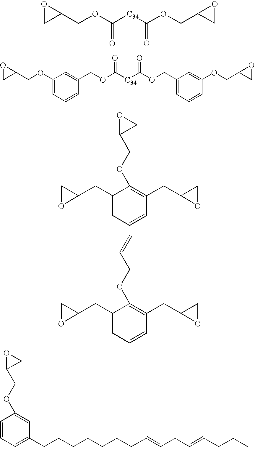
[0003] This invention is an adhesive solution or dilute paste that can be applied to a die or wafer without physically contacting the die or wafer, and be inscripted by a laser for marking or identification. The adhesive solution or paste contains one or more colored fillers and is applied by spraying onto the non-active surface of the wafer or single die. The adhesive can be any adhesive that is currently used under similar fabrication steps for semiconductor packages, although epoxies or electron donor and electron acceptor adhesive systems are preferred. In addition to facilitating laser marking, the adhesive provides mechanical support, and protection from electrostatic shock and light induced bias.

Problems solved by technology

As dies and wafers become thinner, their physical integrity can be compromised by either of these methods; thus, there is a need for a marking medium that can be applied without physically jeopardizing the die or wafer.

Method used


Image

  • Sprayable adhesive material for laser marking semiconductor wafers, dies and devices
  • Sprayable adhesive material for laser marking semiconductor wafers, dies and devices
  • Sprayable adhesive material for laser marking semiconductor wafers, dies and devices

Examples


examples

[0020] Two formulations were prepared as follows: Formulation A contained by weight 23% solid epoxy resin, 9% liquid epoxy resin, 10% phenolic hardener, 0.1% imidazole catalyst, 50% solvent, 0.1% silane adhesion promoter, 6.2% carbon black and 0.1% blue pigment (to enrich the black). Formulation A had a viscosity of 0.58 Pa.s. Formulation B contained by weight 22% solid epoxy resin, 9% liquid epoxy resin, 10% phenolic hardener, 0.5% imine catalyst, 49% solvent, 0.1% silane adhesion promoter, 6% carbon black, 3% titanium dioxide and 0.2% blue pigment. Formulation B had a viscosity of 0.33 Pa.s.

[0021] Formulations A and B were sprayed onto the inactive surface of a five inch silicon wafer using an Asymtek EFD 780S-ss spray head to a thickness of 50 μm. The adhesives were heated on the wafer for 10 minutes at 130° C. to evaporate the solvent and then cured by heating at 150° C. for 30 minutes. The wafer was then diced into four quadrants and each quadrant attached to a lead frame ball...


PUM

PropertyMeasurementUnit
Lengthaaaaaaaaaa
Lengthaaaaaaaaaa
Percent by massaaaaaaaaaa

Abstract

A sprayable adhesive composition having a viscosity within the range of 0.5 Pa.s to 5.0 Pa.s, containing at least one colored filler present in an amount up to 50% by weight of the adhesive composition, is suitable for marking identifications or fiducials on semiconductor dies or wafers. The preferred resins include epoxy resins or combinations of an electron donor resin and an electron acceptor resin.

Description

FIELD OF THE INVENTION [0001] This invention relates to a material for laser marking semiconductor wafers, dies and devices. BACKGROUND OF THE INVENTION [0002] In the fabrication of microelectronic devices, many of the operations are performed using machines with machine-vision technology. Semiconductor dies and packaged semiconductor dies are marked with fiducials and identification marks that are readable by these machines, allowing the dies to be accurately identified and positioned on a chosen substrate, such as a circuit board. A preferred method of marking is to use a laser to inscript the fiducial or identification mark. This can be done on the inactive face of the die, which changes the color of the silicon, or on a marking film applied to the inactive face of the die or wafer. As dies and wafers become thinner, their physical integrity can be compromised by either of these methods; thus, there is a need for a marking medium that can be applied without physically jeopardizin...

Claims


Application Information

Patent Timeline
IPC IPC(8): C08L63/00C09J163/00C09J11/04C09J201/00H01L23/544
CPCC08L63/00C09J11/04C09J163/00H01L23/544H01L2223/54473H01L2924/0002C08L2666/28H01L2924/00
Inventor HE, XIPINGTOMASO, TOREY
Owner HENKEL KGAA
Features
  • R&D
  • Intellectual Property
  • Life Sciences
  • Materials
  • Tech Scout
  • Unparalleled Data Quality
  • Higher Quality Content
  • 60% Fewer Hallucinations
Learn More