Superjunction device with improved ruggedness

a superjunction device and rugged technology, applied in the direction of semiconductor devices, basic electric elements, electrical equipment, etc., can solve the problems of reduced ruggedness and high bv

Active Publication Date: 2005-04-21
SILICONIX TECH C V
View PDF20 Cites 39 Cited by
  • Summary
  • Abstract
  • Description
  • Claims
  • Application Information

AI Technical Summary

Benefits of technology

[0006] The invention proposes a different modification. Instead of using the same design for all the layers, the topmost layer design is modified with a slightly larger feature (diameter) and thus increased volume and P charge, solely in the active area such that the BV of the active area cells is reduced selectively and also so that the current flows into or toward the axis of the P column, thus improving the ruggedness. The lower 5 layers and the termination can then be optimized for maximum BV. The use of the separate upper or 6th layer design will allow the realization of high termination BV, relatively lower active area BV and current flow in the P-column. The conjunction of these 3 factors will improve the ruggedness and increase the process window tolerance since it reduces the dependence of the EAS on the device BV. Note that while a six layer design has been chosen to illustrate the invention, any number of layers can be used.

Problems solved by technology

Exceeding this window on the N-type side leads to high BV but can lead to ruggedness reduction.

Method used


Image

  • Superjunction device with improved ruggedness
  • Superjunction device with improved ruggedness
  • Superjunction device with improved ruggedness

Examples


Embodiment Construction

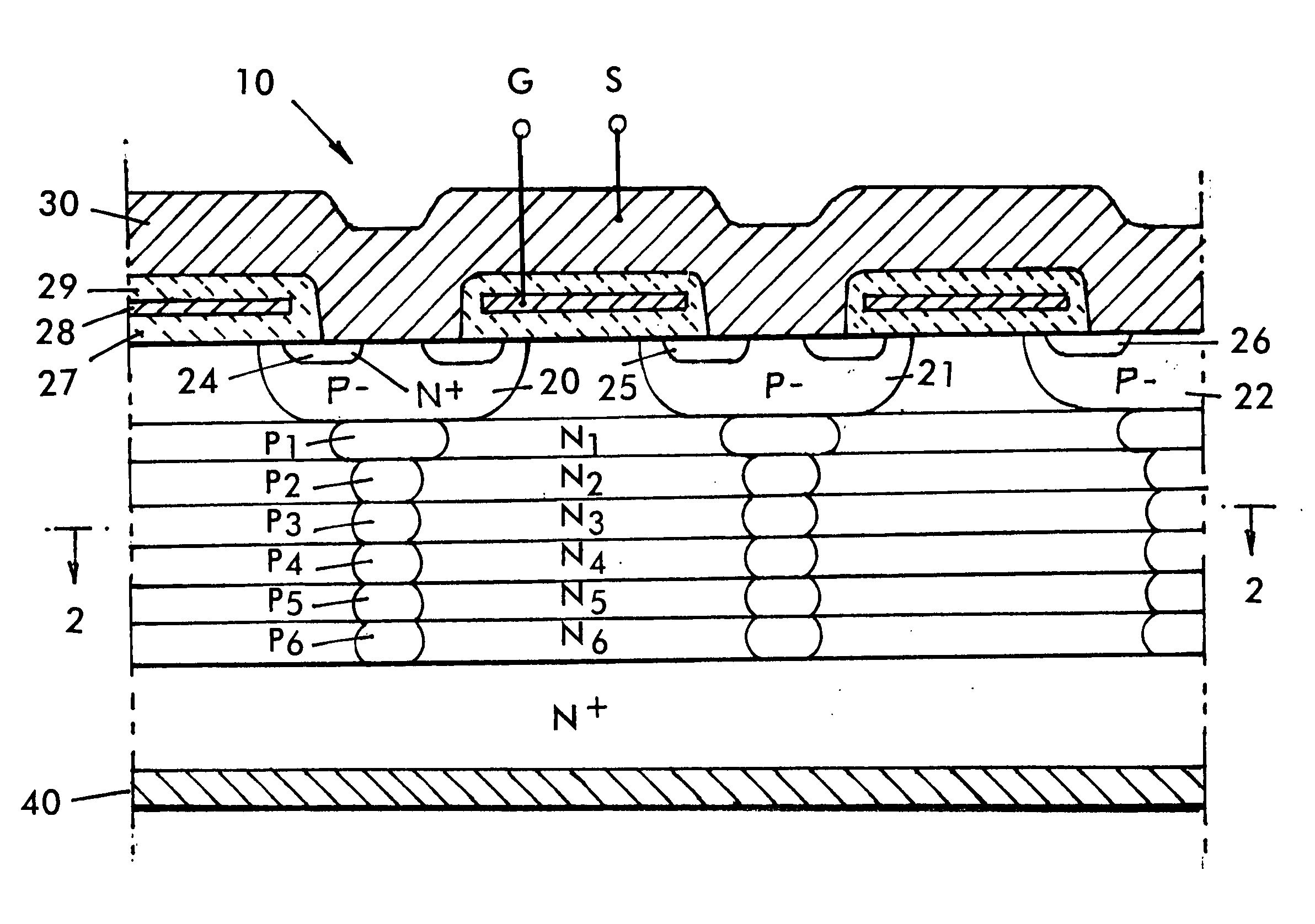
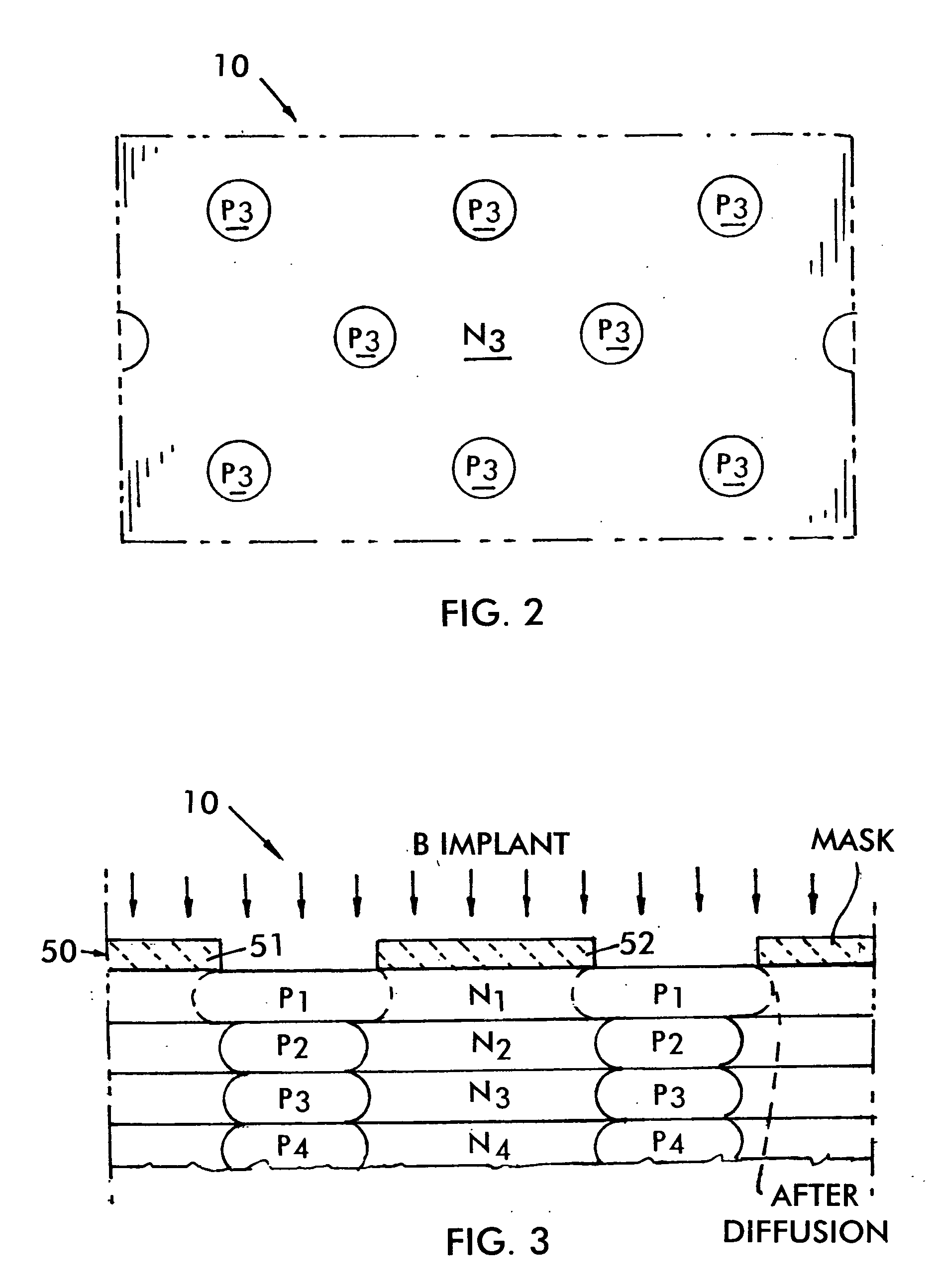
[0010] Referring to FIGS. 1 to 3, a silicon wafer (sometimes referred to as a die or chip) is formed of an N+ wafer 10 which receives a series of epitaxial layers N6 to N1 which are sequentially formed. After the formation of each layer, an implant and diffusion is carried out to form P regions (P6 to P1 respectively). In the prior art, the implant and diffusions are identical in size and concentration and which are charge balanced to the surrounding charge of layers N6 to N1 respectively, which are each of the same concentrations.

[0011] Each of P regions P6 to P1 are aligned to one another to form a continuous column or “pylon”.

[0012] A MOSgated structure is then formed atop each column, shown in FIG. 1 as P channel regions 20, 21 and 22 which conventionally receive N+ source regions 24, 25 and 26 respectively. A gate oxide 27 is deposited over the inversion areas of each of channel regions 20, 21 and 26 respectively and a conductive polysilicon gate 28 is formed over each of gat...


PUM


Abstract

An improved superjunction semiconductor device includes a charged balanced pylon in a body region, where a top of the pylon is large to create slight charge imbalance. A MOSgated structure is formed over the top of the pylon and designed to conduct current through the pylon. By increasing a dimension of the top of the pylon, the resulting device is less susceptible to variations in manufacturing tolerances to obtain a good breakdown voltage and improved device ruggedness.

Description

RELATED APPLICATION [0001] The present application is based on and claims benefit of U.S. Provisional Application No. 60 / 513,174, filed Oct. 21, 2003, entitled Superjunction Device with Improved Ruggedness, to which a claim of priority is hereby made.FIELD OF THE INVENTION [0002] This invention relates to superjunction devices and a process for their manufacture, and more specifically to the increase of the ruggedness of superjunction devices, and the increase of the process window tolerances for such devices. BACKGROUND OF THE INVENTION [0003] Superjunction devices possess the advantage of significantly reduced Rdson for the same high breakdown voltage (BV) of a conventional MOSFET. The superjunction is comprised of a multi-layer, for example, a six-layer sequence of implant and epitaxy to form spaced P-columns which is used to balance the charge in the N type drift region epi which receives the columns. The same reticle is used repetitively on the six layers to generate the P-colu...

Claims


Application Information

Patent Timeline
Patent Type & Authority Applications(United States)
IPC IPC(8): H01L29/06H01L21/306H01L21/332H01L21/336H01L29/10H01L29/78
CPCH01L29/0634H01L29/1095H01L29/66712H01L29/7802H01L2924/0002H01L2924/00H01L21/38
Inventor SRIDEVAN, SRIKANT
Owner SILICONIX TECH C V
Why Eureka
Try Eureka