CMOS image sensor and manufacturing method thereof

a technology of image sensor and manufacturing method, which is applied in the direction of electrical equipment, semiconductor devices, radio frequency controlled devices, etc., can solve the problem that metal is likely to be eroded by the developer solution

Inactive Publication Date: 2005-04-21
COLUMBA TECH INC
View PDF9 Cites 11 Cited by
  • Summary
  • Abstract
  • Description
  • Claims
  • Application Information

AI Technical Summary

Benefits of technology

[0010] The present invention has been made in an effort to solve the above problems, and it is an object of the present invention to provide a CMOS image sensor which is capable of protecting the previously formed color filter during the color filter formation rework, by forming isolation layer(s) between the color filters.

Problems solved by technology

Also, since the color filter-forming processes should be carried out three times or more while the metal on the pad part is exposed such that the metal is likely to be eroded by the developer solution.
The damage of the metal pad causes various problems in wire bonding and probe test processes.

Method used


Image

  • CMOS image sensor and manufacturing method thereof
  • CMOS image sensor and manufacturing method thereof
  • CMOS image sensor and manufacturing method thereof

Examples


first embodiment

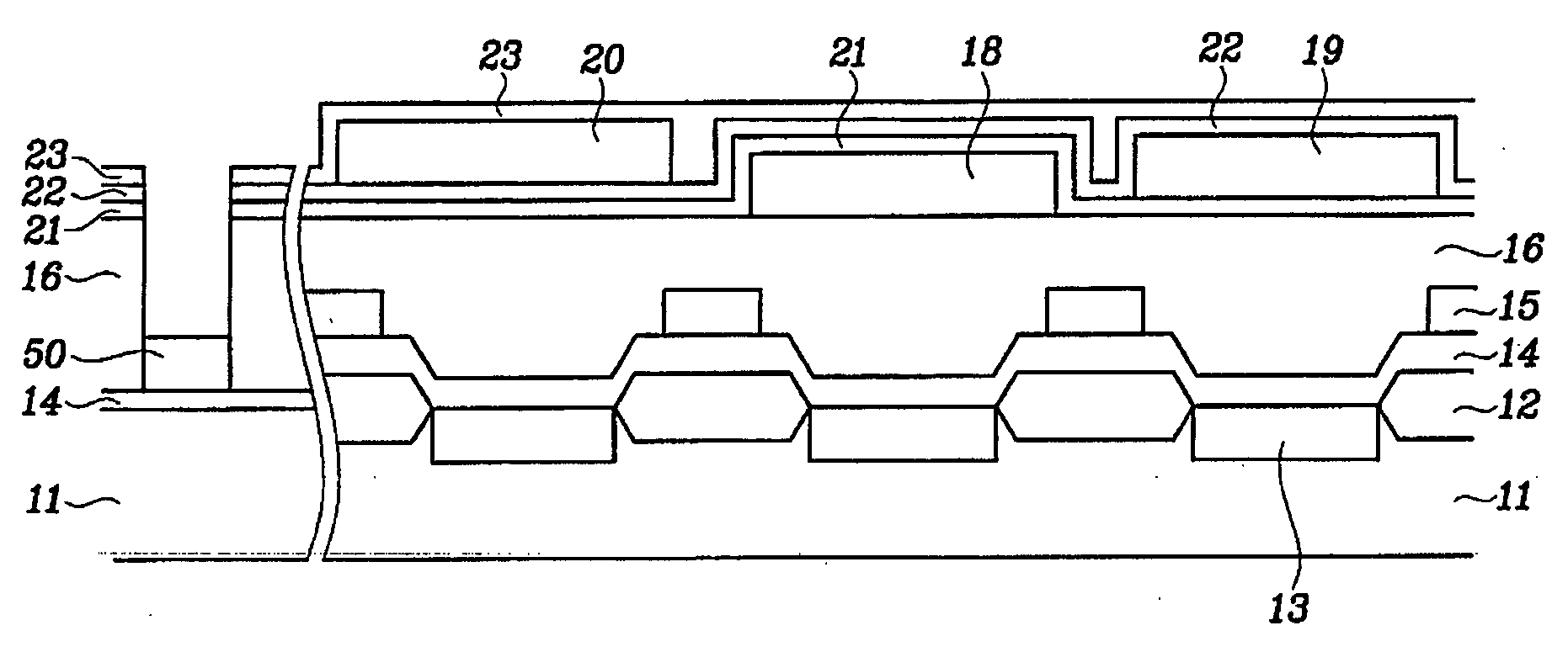
[0027]FIG. 1 is a cross-section view illustrating a CMOS image sensor according to the present invention

[0028] Referring to FIG. 1, the CMOS image sensor according to the first embodiment of the present invention includes a field oxide layer 12 formed on a semiconductor substrate 11 for electrically isolating the devices from each other. On the semiconductor substrate 11, a gate electrode (not shown) of a transistor, made by depositing polysilicon and tungsten silicide, is formed.

[0029] And, a light receiving area comprised of photodiodes 13 is formed in the semiconductor substrate 11 and a source and a drain of the transistor and a sensing node (not shown) are formed by ion implanting.

[0030] Also, on the semiconductor substrate 11, an interlayer insulating film 14 and metal wiring 15 are sequentially formed, and a pad part 50 is formed with the metal wiring from the same layer, the metal wiring being connected to an exterior circuit. A protection layer 16 is formed on the metal w...

second embodiment

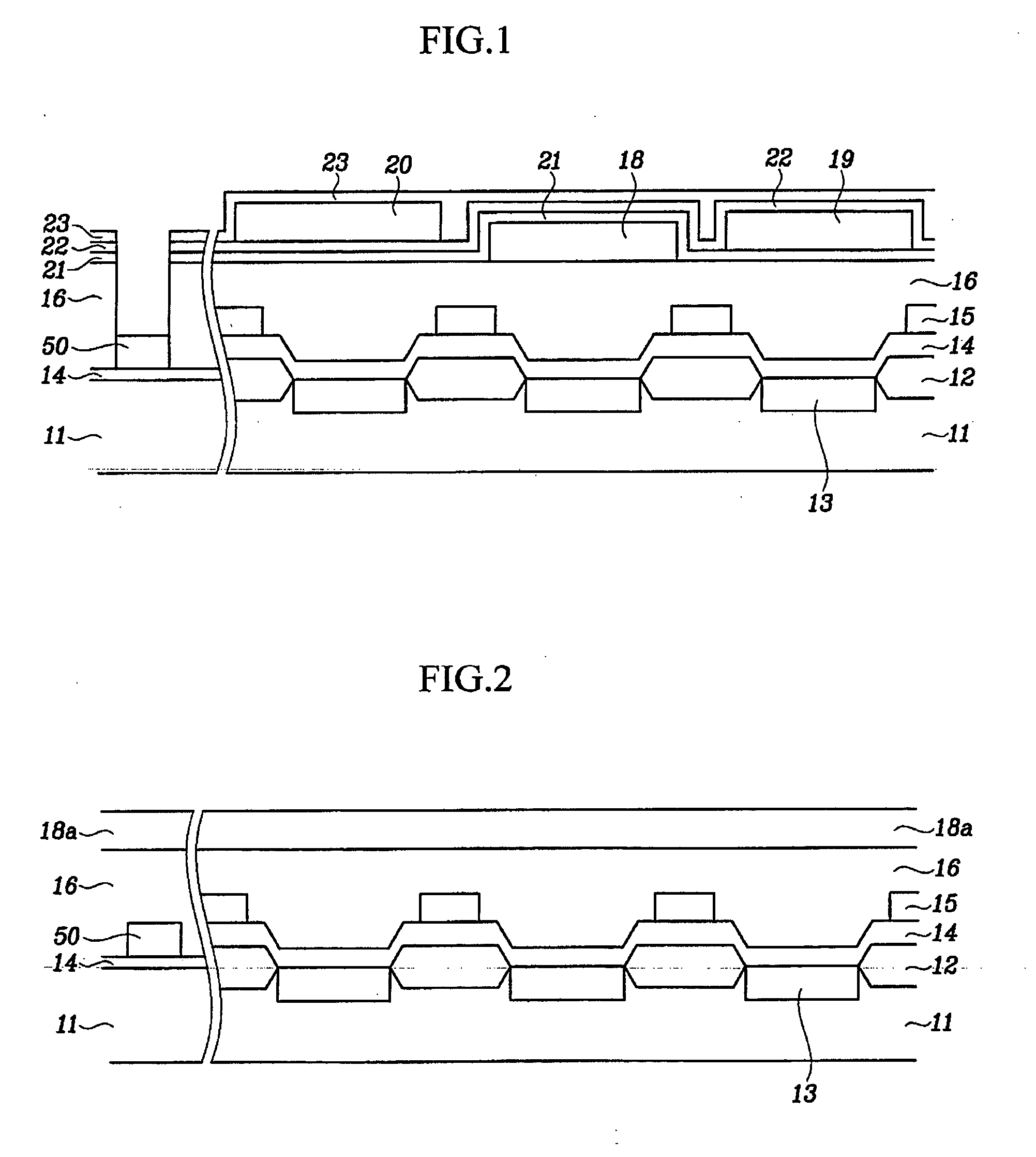
[0056]FIG. 10 is a cross-sectional view illustrating a CMOS image sensor according two the present invention. Here, the identical reference numerals refer to the similar functions and members in the previous drawings.

[0057] As shown in FIG. 10, the blue filter 18 is formed on the protection layer 16, and the first isolation layer 21 is formed on the blue color filter 18 and the protection layer 16. Also, the red filter 19 and the green filter 20 are formed on the first isolation layer 21 so as not to be overlapped with the blue color filter 18 and from each other. In this manner, the process can be simplified by skipping the second isolation layer formation process. Also, by canceling the formation of the second isolation layer which is formed by depositing the thermal oxide layer, it is possible to minimize the performance degradation of the image sensor caused by the heat generated during the thermal oxide layer formation process.

[0058] Also, the third isolation layer 23 is forme...


PUM


Abstract

A CMOS image sensor according to the present invention includes a substrate having a light receiving region, an interlayer insulating film formed on the substrate, a plurality of metal wirings formed on the interlayer insulating film so as to expose the light receiving region, a protection layer coated on the metal wirings and the interlayer insulating film, and a plurality of color filters formed on the protection layer, wherein at least one of the color filters is provided with an isolation layer formed on an upper surface thereof.

Description

BACKGROUND OF THE INVENTION [0001] (a) Field of the Invention [0002] The present invention relates to a CMOS image sensor and a manufacturing method thereof. [0003] (b) Description of the Related Art [0004] An image sensor is a semiconductor device converting optical images into electrical signals and, typically manufactured in a type of a charge coupled device (CCD) or a complementary metal oxide semiconductor (CMOS) image sensor. [0005] The charge coupled device is an integrated circuit containing an array coupled capacitors. Each capacitor stores and transfers electric charge to on or other of its neighbors. In the meantime, the CMOS image sensor is a device adopted a switching mechanism sequentially detecting output using MOS transistors as many as the number of pixels with the CMOS technology which uses the control circuit and signal processing circuit as peripheral devices. [0006] The CMOS image sensor is comprised of a photo-sensing region for detecting the light, a logic cir...

Claims


Application Information

Patent Timeline
Patent Type & Authority Applications(United States)
IPC IPC(8): H01L29/768H01L27/146
CPCH01L27/14621H01L27/14685H01L27/14636H01L27/146
Inventor JANG, HOON
Owner COLUMBA TECH INC
Why Eureka
Try Eureka