Semiconductor device manufacturing method

a manufacturing method and semiconductor technology, applied in the direction of individual semiconductor device testing, semiconductor/solid-state device testing/measurement, instruments, etc., can solve the problems of low efficiency, solder ball position is erroneously recognized, solder ball deformation, etc., and achieve the effect of increasing the reliability of bonding

Inactive Publication Date: 2005-04-21
CASIO COMPUTER CO LTD
View PDF2 Cites 27 Cited by
  • Summary
  • Abstract
  • Description
  • Claims
  • Application Information

AI Technical Summary

Benefits of technology

[0008] It is an object of the present invention to provide a semiconductor device manufacturing method which can execute burn-in without deforming solder balls so that burn-in can reliably be executed, and the bonding reliability can be increased.
[0010] According to the method, before formation of the solder balls, burn-in is executed for the semiconductor substrate in a wafer state while bringing the probe pins into contact with the upper surfaces of the columnar electrodes. Hence, any unwanted deformation of the solder balls by contact of the probe pins can be prevented. As a result, burn-in can reliably be executed, and the bonding reliability can be increased.

Problems solved by technology

In this case, the efficiency is low because burn-in is executed for semiconductor devices diced into individual devices.
However, when the probe pins come into contact with relatively soft solder balls, the solder balls may deform.
Because of this deformation, the positions of the solder balls are erroneously recognized by an alignment camera.
When such a semiconductor device is jointed to a circuit board, alignment failures may occur, and accordingly, bonding failures may occur.
For this reason, failures occur in contact between the probe pins and the solder balls so that no appropriate burn-in is executed for some devices.

Method used


Image

  • Semiconductor device manufacturing method
  • Semiconductor device manufacturing method
  • Semiconductor device manufacturing method

Examples


Embodiment Construction

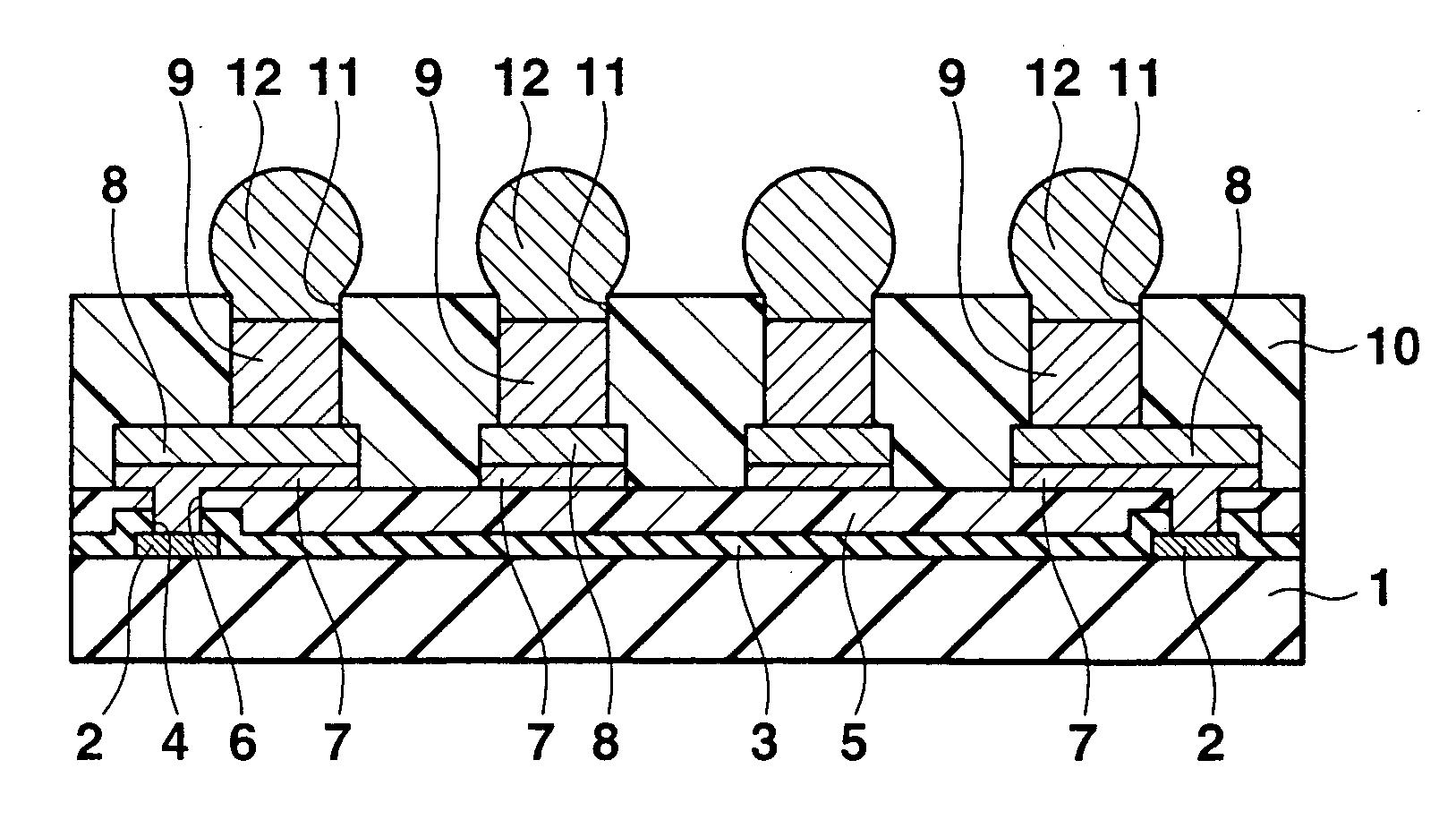
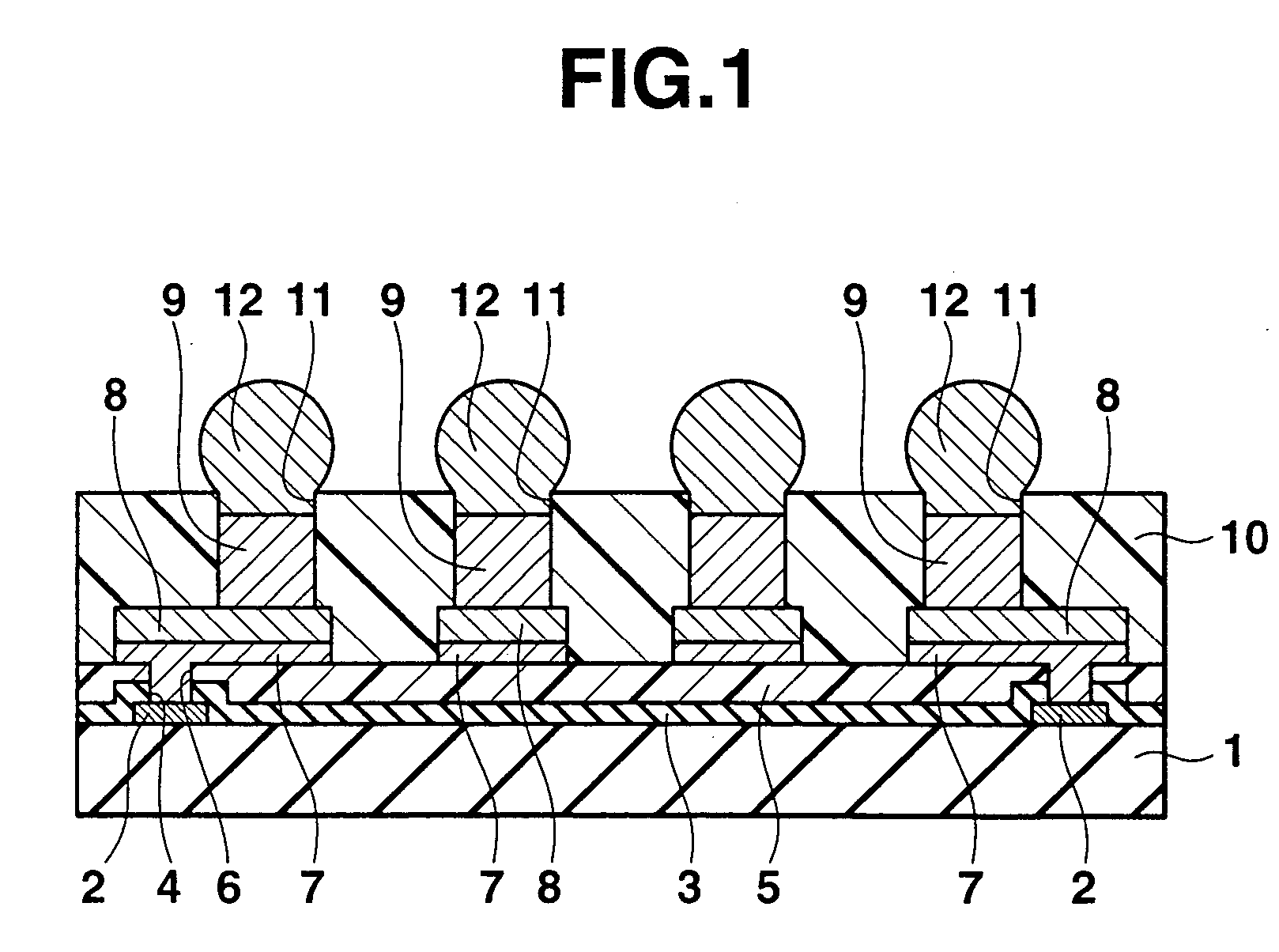
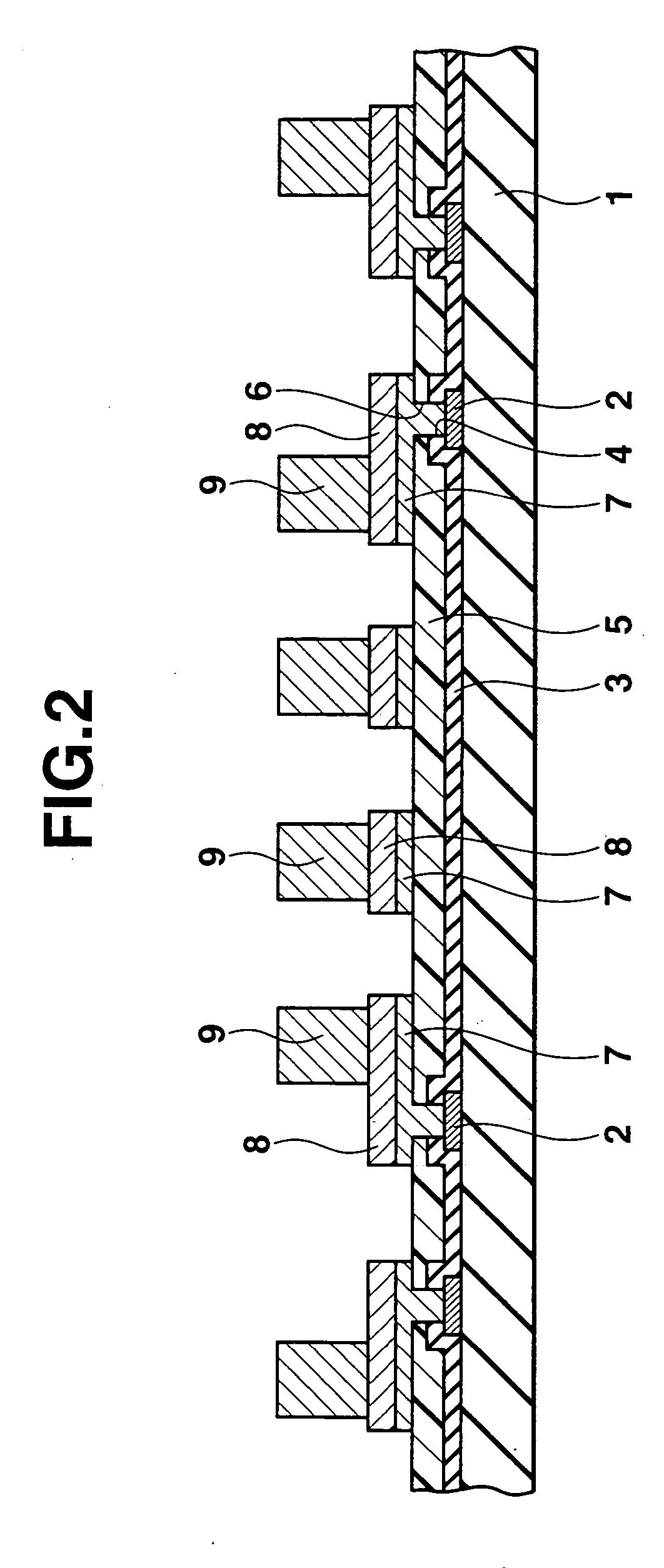
[0021]FIG. 1 is a sectional view of a semiconductor device manufactured by a manufacturing method according to an embodiment of the present invention. This semiconductor device comprises a semiconductor substrate or wafer 1 made of, for example, silicon. An integrated circuit (not shown) having a predetermined function is arranged on the upper surface of the semiconductor substrate 1. A plurality of connection pads 2 made of an aluminum-based metal are formed at the peripheral portion of the upper surface and electrically connected to the integrated circuit. An insulating film 3 made of silicon oxide is formed on the upper surface of the semiconductor substrate 1 except the central portions of the connection pads 2. The central portions of the connection pads 2 are exposed through opening portions 4 formed in the insulating film 3.

[0022] A protective film (insulating film) 5 made of epoxy resin or polyimide resin is formed on the upper surface of the insulating film 3. In this case...


PUM


Abstract

After columnar electrodes and a sealing film are formed above a semiconductor substrate in a wafer state, probe pins are brought into contact with the upper surfaces of the columnar electrodes, and burn-in is executed. Next, solder balls are formed on the columnar electrodes, and the semiconductor substrate in a wafer state is diced. As a result, any unwanted deformation of the solder balls by contact of the probe pins can be prevented. In addition, even when the heights of the solder balls vary, burn-in can be performed.

Description

CROSS-REFERENCE TO RELATED APPLICATIONS [0001] This application is based upon and claims the benefit of priority from prior Japanese Patent Application No. 2003-354680, filed Oct. 15, 2003, the entire contents of which are incorporated herein by reference. BACKGROUND OF THE INVENTION [0002] 1. Field of the Invention [0003] The present invention relates to a semiconductor device manufacturing method. [0004] 2. Description of the Related Art [0005] In the field of semiconductor technology such as LSIs, burn-in is done to guarantee the reliability. Conventionally, semiconductor devices which have been diced into individual devices are subjected to burn-in (e.g., Jpn. Pat. Appln. KOKAI Publication No. 2003-282814). In this case, the efficiency is low because burn-in is executed for semiconductor devices diced into individual devices. [0006] On the other hand, there are semiconductor devices generally called CSP (Chip Size Package) (e.g.,. Pat. Appln. KOKAI Publication No. 2002-231854). ...

Claims


Application Information

Patent Timeline
Patent Type & Authority Applications(United States)
IPC IPC(8): H01L21/66G01R31/28H01L21/56H01L23/12H01L23/31H01L23/485
CPCG01R31/2863G01R31/2886H01L24/13H01L2924/014H01L2924/01006H01L2924/00013H01L2924/14H01L23/3114H01L24/10H01L2224/13022H01L2224/131H01L2924/01013H01L2924/01015H01L2924/01029H01L2924/01033H01L2924/01078H01L2924/01079H01L2924/01082H01L2224/13099H01L2924/00H01L24/05H01L2224/023H01L2224/05008H01L2224/05022H01L2224/05024H01L2224/05124H01L2224/05147H01L2224/05569H01L2224/05571H01L2224/05647H01L2224/13H01L2924/00014H01L2924/0001H01L22/00
Inventor WAKABAYASHI, TAKESHIMIHARA, ICHIRO
Owner CASIO COMPUTER CO LTD
Why Eureka
Try Eureka