
Organic thin film transistor array substrate and method of producing the same

a technology of organic thin film transistors and array substrates, which is applied in the direction of transistors, optics, instruments, etc., can solve the problems of unsatisfactory electrical properties, complex process, and unsatisfactory and achieve the effect of improving the electrical properties of o

Inactive Publication Date: 2005-04-28
IND TECH RES INST
View PDF1 Cites 0 Cited by
  • Summary
  • Abstract
  • Description
  • Claims
  • Application Information

AI Technical Summary

Benefits of technology

The solution improves the electrical properties of OTFTs to meet circuit design requirements while simplifying the production process by aligning organic semiconductor materials effectively, thereby enhancing carrier transport efficiency and reducing process complexity.

Problems solved by technology

In this method, OTFT exhibits unsatisfactory electric properties and there is no LC alignment film.
However, the organic semiconductor in the OTFT not control the alignment, thus the electrical properties are unsatisfactory and the process is more complicated.
In the above-mentioned OTFT and LCD integrated elements, the organic semiconductor of the OTFT is not aligned; therefore electrical properties are not satisfactory and do not meet circuit design requirements.
Additionally, if compatible OTFT and LCD processes are not utilized properly, process complexity increases.

Method used


Image

  • Organic thin film transistor array substrate and method of producing the same
  • Organic thin film transistor array substrate and method of producing the same
  • Organic thin film transistor array substrate and method of producing the same

Examples


first embodiment

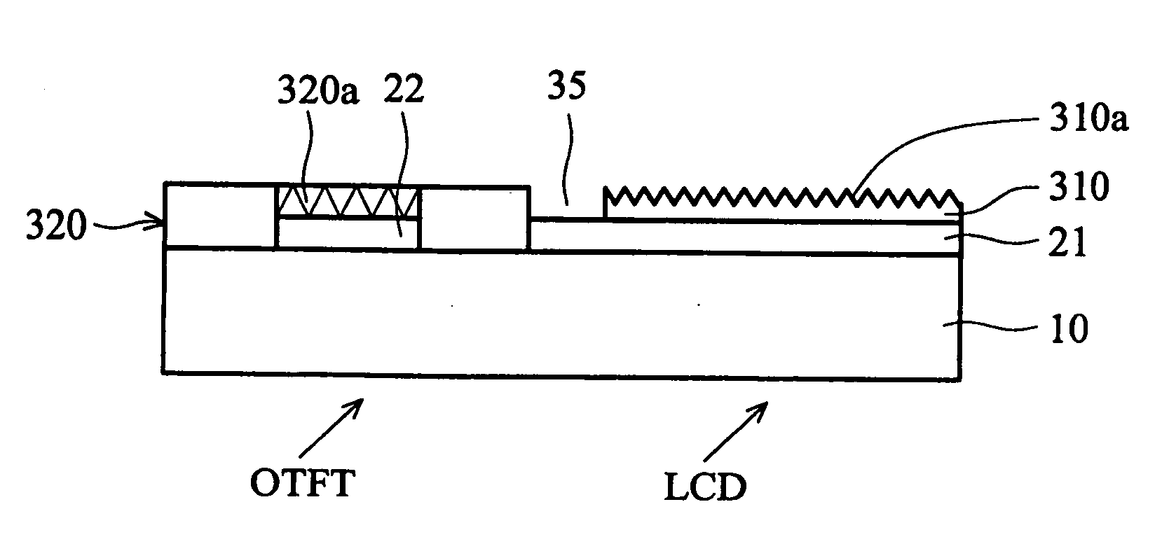
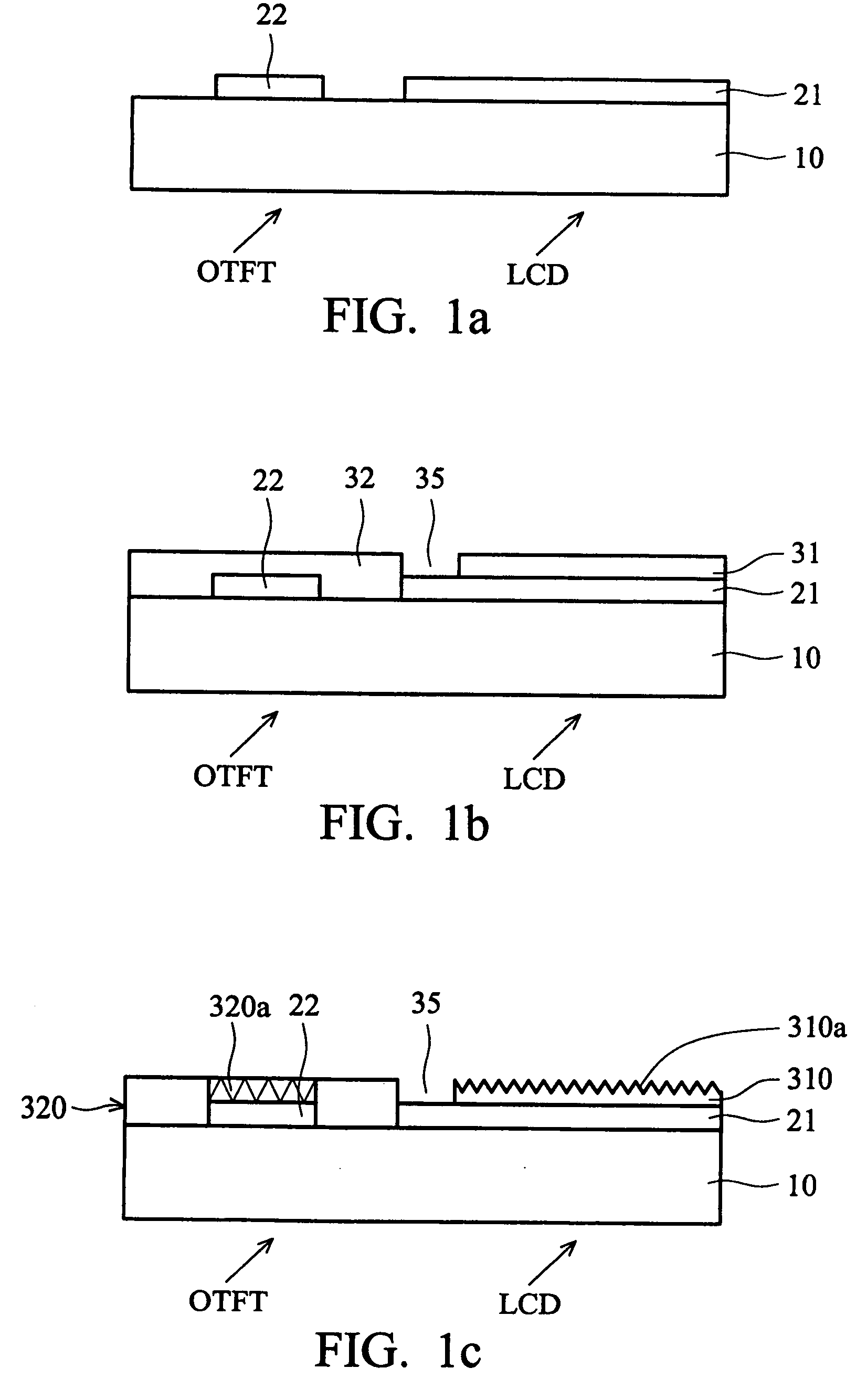
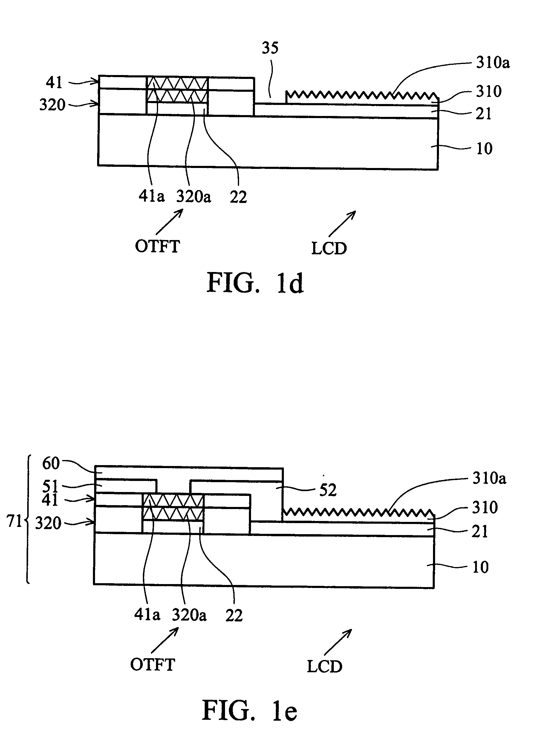
[0022]FIGS. 1a˜1f illustrate cross sections of the method for producing an LCD having a bottom gate type OTFT substrate according to the invention.

[0023] In FIG. 1a, a substrate 10 having LCD and OTFT areas is provided. Suitable substrates are silicon wafer, glass, and quartz, plastic or flexible substrates. A transparent conductive layer (not shown), preferably ITO, ZnO or conductive polylmer material, is formed on the substrate 10. The transparent conductive layer is then patterned by photolithography, or etching to form a pixel electrode 21 in the LCD area and a gate 22 in the OTFT area. Alternatively, printing is also applicable to form the pixel electrode 21 and the gate 22 directly.

[0024] Next, in FIG. 1b, a dielectric layer (not shown) is formed in the LCD area and the OTFT area to cover the pixel electrode 21 and the gate 22. Then, the dielectric layer is patterned to form an opening 35, wherein the dielectric layer is divided into two parts: a first dielectric layer 31 on ...

second embodiment

[0035]FIG. 2 illustrates a cross section of the LCD having a bottom gate type OTFT array substrate according to the invention. This LCD comprises: an OTFT array substrate 72, a color filter 75, and liquid crystal 80 between the OTFT array substrate 72 and the color filter 75.

[0036] The OTFT array substrate 72 in FIG. 2 comprises: a substrate 10 having an LCD area and an OTFT area; a transparent pixel electrode 21, formed on the substrate 10 in the LCD area; a gate 22, formed on the substrate 10 in the OTFT area; a first alignment film 310, formed on the pixel electrode 21; a second alignment film 330, formed on the substrate 10 in the OTFT area and covering the gate 22; an organic semiconductor layer 42, formed on the second alignment film 330, wherein the organic semiconductor layer 42 is aligned along the direction of the second alignment film 330; and a source 51 and a drain 52, formed in the OTFT area, wherein the source and the drain are in contact with the organic semiconducto...

third embodiment

[0044]FIGS. 3a˜3f illustrate cross sections of the method of producing an LCD having a top gate type OTFT array substrate according to the invention.

[0045] In FIG. 3a, a substrate 10 having an LCD and OTFT areas is provided. Suitable substrates are silicon wafer, glass, and quartz, plastic or flexible substrates. A pixel electrode 25, preferably ITO, ZnO or conductive polymer material, is formed on the substrate 10 in the LCD area.

[0046] Next, in FIG. 3b, a dielectric layer (not shown) is formed in the LCD area and the OTFT area to cover the pixel electrode 25. Then, the dielectric layer is patterned and divided into two parts: a first dielectric layer 37 on the pixel electrode 25 and a second dielectric layer 38 on the substrate in the OTFT area. Patterning of the dielectric layer is carried out by photolithography and etching. Or, printing is also applicable in forming the first dielectric layer 37 and the second dielectric layer 38 directly.

[0047] Next, in FIG. 3c, the first di...


PUM

PropertyMeasurementUnit
areaaaaaaaaaaa
transparentaaaaaaaaaa
anisotropicaaaaaaaaaa

Abstract

The invention provides an organic thin film transistor array substrate, comprising: a substrate, having a liquid crystal display area and an organic thin film transistor area; a pixel electrode, formed on the substrate in the LCD area; a first alignment film, formed on the pixel electrode; a second alignment film, formed on the substrate in the OTFT area; an organic semiconductor layer, formed on the second alignment film, wherein the organic semiconductor layer is aligned along the direction of the second alignment film; and a gate, a source and a drain, formed in the OTFT area, wherein the source and the drain are in contact with the organic semiconductor layer and a channel is formed between the source and the drain.

Description

BACKGROUND OF THE INVENTION [0001] 1. Field of the Invention [0002] The invention provides an organic thin film transistor array substrate, and in particular, an organic thin film transistor array substrate having an alignment film, formed in the same process step using the same material, in the OTFT area and the LCD area. [0003] 2. Description of the Related Art [0004] Organic semiconductor material has been lauded by many international research institutes, as one of the most promising materials for producing thin film transistors and other electronic and optic-electro elements. Sirringhaus etc. of the University of Cambridge, discloses the process of producing OTFT by self-organization of organic molecules to obtain alignment of various anisotropic structures. Better alignment of the molecular chain results in enhanced electric charge transportation efficiency. Carrier mobility of the transistor increases at least 100 times, thereby proving that the alignment of organic molecules ...

Claims


Application Information

Patent Timeline
Patent Type & Authority Applications(United States)
IPC IPC(8): G02F1/1335G02F1/1337G02F1/1368H01L21/00H01L21/336H01L29/786H10K99/00
CPCG02F1/133555G02F1/13378H01L51/0545H01L27/28H01L51/0541G02F1/1368H10K19/00H10K10/466H10K10/464
Inventor CHENG, HORNG-LONGCHOU, WEI-YANGWONG, YIH-JUNWANG, YU-WULEE, CHENG-CHUNG
Owner IND TECH RES INST
Learn More