Capacity load type probe, and test jig using the same

a probe and load technology, applied in the field of capacity load probes, can solve the problems of inaccurate measurement, power supply voltage change, and the probe in the metal block b>1/b> tends to pick up noise in the high frequency/high speed device, so as to avoid noise, remove rf noise, and test precise

Inactive Publication Date: 2005-04-28
YOKOWO CO LTD
View PDF10 Cites 9 Cited by
  • Summary
  • Abstract
  • Description
  • Claims
  • Application Information

AI Technical Summary

Benefits of technology

[0016] In such a structure, because a capacitor which bypasses RF noise is formed to the peripherals at least one of the power supply and signal probes, RF noise can be bypassed just before the probes contact the power supply terminal and the signal terminal of the DUT. The capacitor can not only avoid noise, but also remove RF noise which remains on the side of the wiring board (printed circuit board). As a result, noise from the power supply and medium/low frequency signal probes having the movable pins for contact with the DUT is completely removed, achieving a precise test without influence of noise. Additionally, by using the capacity loaded probe as the power supply probe, a voltage drop at the power supply terminal caused by a current change in the DUT can be reduced to within 10 percent of a general

Problems solved by technology

In even such a structure, however, the probe in the metal block 1 tends to pick up noise in the high frequency/high speed device.
On the other hand, when the power supply terminal 23 picks up high frequency/high speed noise, it causes power supply voltage to change, an amplifier to oscillate, so it causes inaccurate measurement.
A precise test cannot be achieved when RF noise is input to the signal terminals for medium or low frequency signals.
Thus, a precise test cannot be achieved.
Consequently, the number of the terminals (electrodes) is increased, and pitches between the terminals are shortened, so that noise tends to be superimposed

Method used


Image

  • Capacity load type probe, and test jig using the same
  • Capacity load type probe, and test jig using the same
  • Capacity load type probe, and test jig using the same

Examples


Embodiment Construction

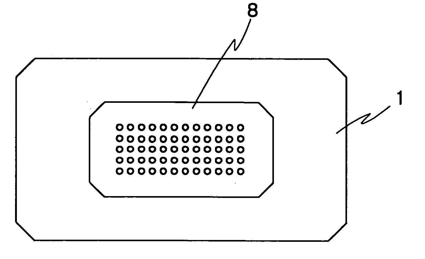
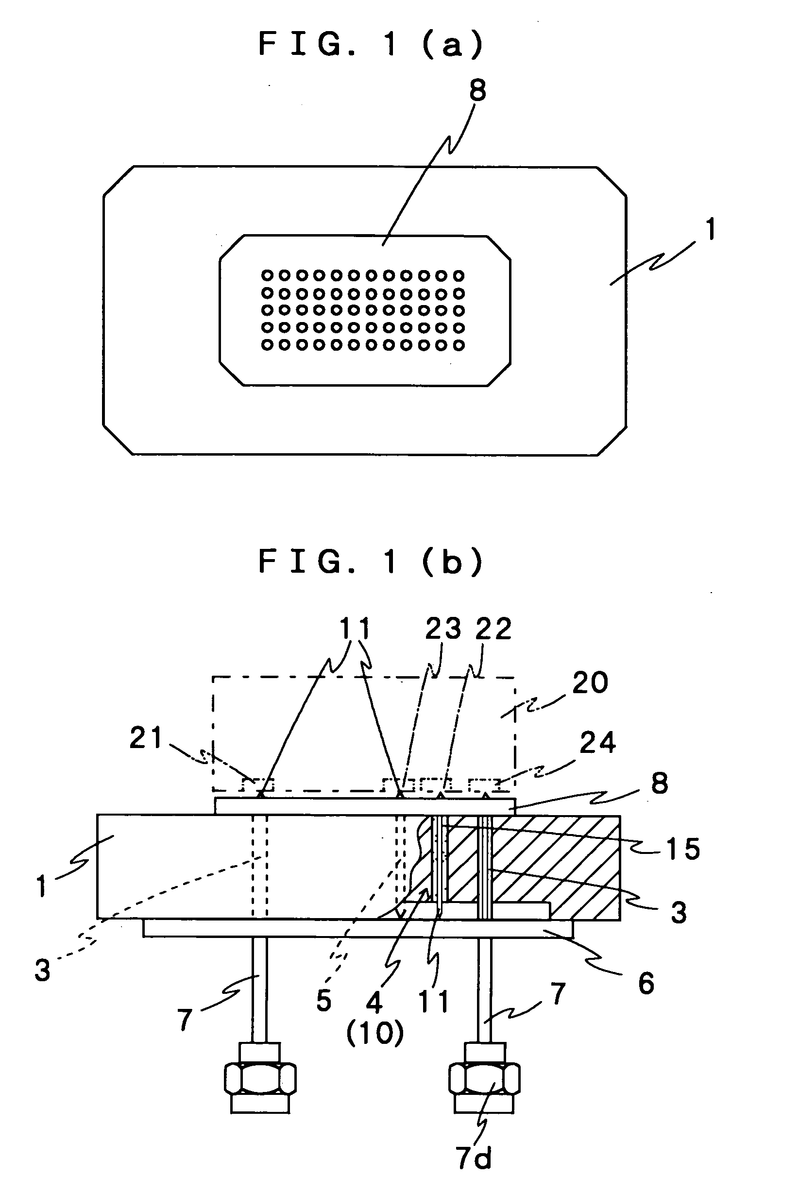
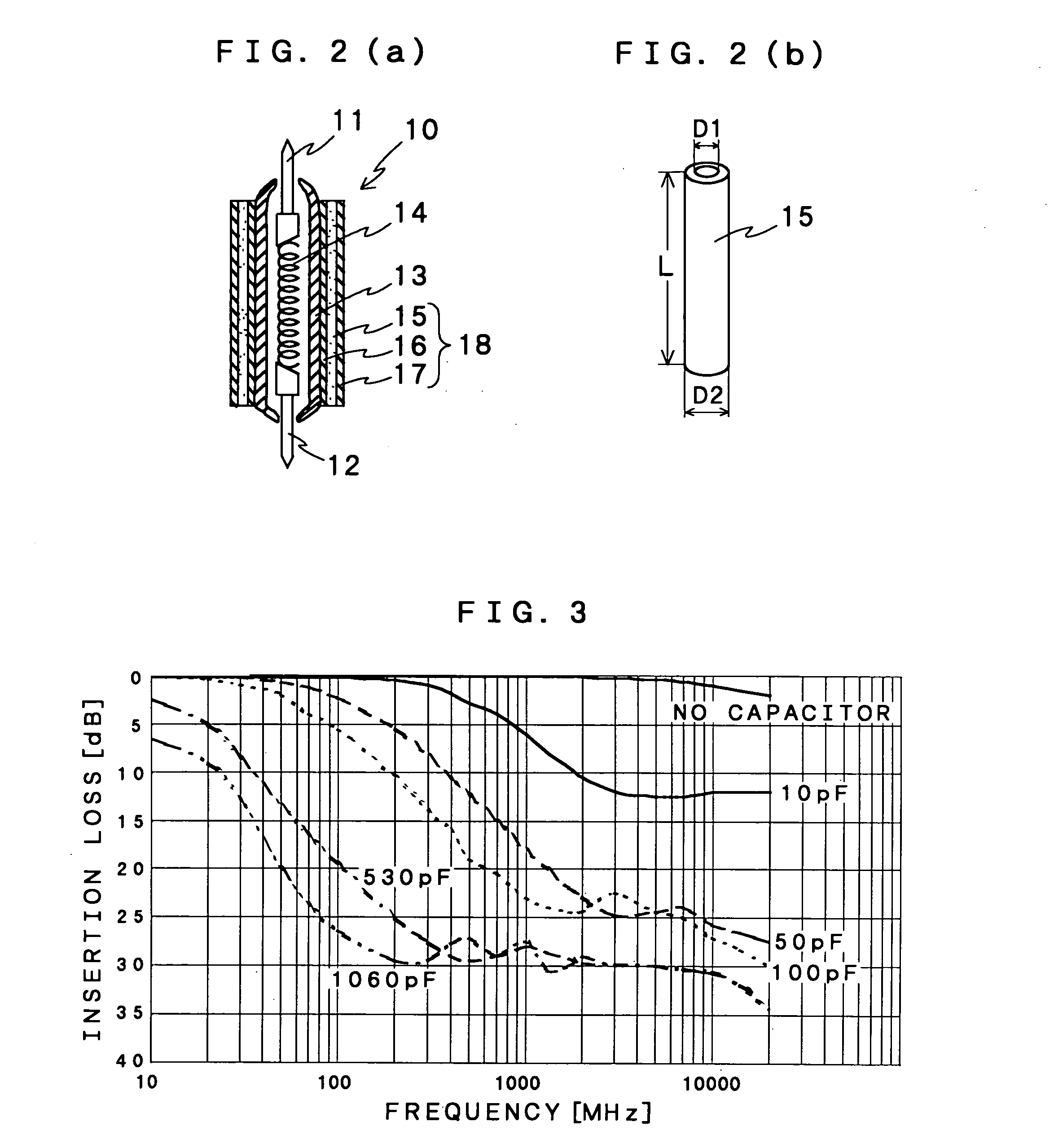
[0031] Next, a capacity loaded probe of the present invention and a test jig using the probe will be explained in the following in reference with the drawings. The test jig of the present invention connects between a DUT 20 and a test apparatus (not shown). As shown in the top view and partial sectional views of FIGS. 1(a), (b), a plurality of probes such as a signal probe 3, power supply probe 4, and ground probe 5 are provided into a metal block 1 so as to penetrate. Each of the probes has a movable pin 11. A tip of the movable pin 11 is projecting from one surface of the metal block 1. A projection length of the tip is variable. The DUT 20 is pressed onto the one surface of the metal block 1. Each of electrode terminals 21 to 24 of the DUT 20 contacts the tips of the probes 3 to 5 to test characteristics of the DUT 20. In this invention, at least a part of the probes is capacity loaded probe whose outer circumferential surface is provided with dielectric layer and metal film to f...


PUM


Abstract

A plurality of probes such as a signal probe (3) and a power supply probe (4) are provided into a metal block (1) so as to penetrate. Each of the probes has a movable pin (11). A tip of the movable pin is projecting from one surface of the metal block (1). And a projection length of the tip is variable. A DUT 20 is pressed onto the surface of the metal block (1) to contact between electrode terminals (21 to 24) and tips of the probes to test characteristics of the DUT. At least one of the probes is capacity loaded probe having a capacitor by providing a dielectric layer and a metal film to peripheral of the probe. As a result, noise can be removed reliably. Additionally, when the capacity loaded probe is used as the power supply probe, a voltage drop is reduced at the power supply terminal in a case of change of the output.

Description

TECHNICAL FIELD [0001] The present invention relates to a capacity loaded probe where, for example in testing a high frequency / high speed device (hereinafter high frequency means the frequency is high in analog and high speed means digital signal having a small pulse width or small pulse separation) such as a semiconductor wafer, IC, or module for an amplification circuit and mixer circuit built in, e.g., a cellular phone, reliable contact between the DUT (Device Under Test) and a test apparatus is achieved to reduce influence of external noise to the minimum, and to a test jig using the capacity loaded probe. BACKGROUND ART [0002] For example, to solve the problem that an exposed lead tends to pick up noise in testing a high frequency / high speed device such as a semiconductor wafer, IC, or module, a structure where electrode terminals 21 to 23 of a DUT 20 are connected to a test jig which contains an RF (this term means high frequency and high speed) signal probe 3, power supply pr...

Claims


Application Information

Patent Timeline
IPC IPC(8): G01R1/067
CPCG01R1/06772G01R1/06722
Inventor YANAGISAWA, WASUKENAKAKOJI, MAKOTOHORIE, RYOYOSHIDA, TAKUTO
Owner YOKOWO CO LTD
Why Eureka
Try Eureka