Structure for reducing leakage currents and high contact resistance for embedded memory and method for making same

a technology of leakage current and embedded memory, which is applied in the direction of semiconductor devices, semiconductor/solid-state device details, electrical apparatus, etc., can solve the problems of difficult to make contacts to shallow diffused junctions for fets without overetching, affecting the efficiency of etching, and alignment problems on integrated circuits having 0.1 micron (um) minimum feature sizes, etc., to achieve more relaxed alignment tolerances and alignment tolerances

Active Publication Date: 2005-05-05
TAIWAN SEMICON MFG CO LTD
View PDF21 Cites 204 Cited by
  • Summary
  • Abstract
  • Description
  • Claims
  • Application Information

AI Technical Summary

Benefits of technology

[0016] The method by a second embodiment is described for making contact openings of varying depths in an insulating layer on a substrate for merged logic / memory having trench capacitors. The method begins similar to the first embodiment up to and including the formation of the shallow trench isolation. After forming the trench isolation, semiconductor devices, such as FETs, are formed in device areas. Next, recesses are formed in the shallow trench isolation in the memory regions (RAM) for trench capacitors. A conformal first conducting layer is deposited and patterned to form capacitor bottom electrodes in the recesses. A stacked layer comprised of an interelectrode dielectric layer, a second conducting layer, and an anti-reflective coating (ARC) is deposited over the bottom electrodes. The stacked layer is patterned to form capacitor top electrodes from the second conducting layer. A key feature is to form open areas in the stacked layer during patterning of the top electrodes. During patterning the sidewalls of the second conducting layer are exposed within the open areas. An insulating layer is deposited on the substrate and over the top electrodes having the ARC. The insulating layer is planarized. Another key feature is to use a novel mask design and a single masking step to etch contact openings of varying depths in the planar insulating layer for contacts to the FETs on the substrate and, in the memory regions (RAM), concurrently etching contact openings extending over and along the edge of the top electrodes in the open areas to expose the second conducting layer. This etching step allows one to etch contact openings to the substrate without overetching, while providing a means for forming contacts having low-contact resistance to the sidewalls of the top electrodes. Another feature of the mask design is to form a series of contact openings, for example, two contact openings are etched over the edge of the patterned second conducting layer in the open areas on opposite sides of the open areas to allow for more relaxed alignment tolerances. Another method is to form a series of contact openings that are skewed along the edges of the patterned second conducting layer on opposite sides of the open areas to also provide for more relaxed alignment tolerances. Further, a series of contact openings that are elongated normal to the edge of the patterned second conducting layer can be formed to also relax the alignment tolerances.

Problems solved by technology

However, when a single masking step is used, it is difficult to make contacts to shallow diffused junctions for the FETs without overetching, while concurrently forming low-electrical-resistance contacts to the DRAM capacitor.
The conventional process that utilizes two separate masking and etching steps is not cost-effective and can cause alignment problems on integrated circuits having 0.1 micron (um) minimum feature sizes.
This problem also arises for conventional trench capacitors as depicted in FIG. 2.
However, there is still a need in the semiconductor industry to provide a process for making logic circuits with embedded DRAM devices using a single mask for etching contact openings of varying depths without resulting in high contact resistance to capacitor top electrodes and high leakage currents to shallow diffused junctions on / in the substrate surface.

Method used


Image

  • Structure for reducing leakage currents and high contact resistance for embedded memory and method for making same
  • Structure for reducing leakage currents and high contact resistance for embedded memory and method for making same
  • Structure for reducing leakage currents and high contact resistance for embedded memory and method for making same

Examples


Embodiment Construction

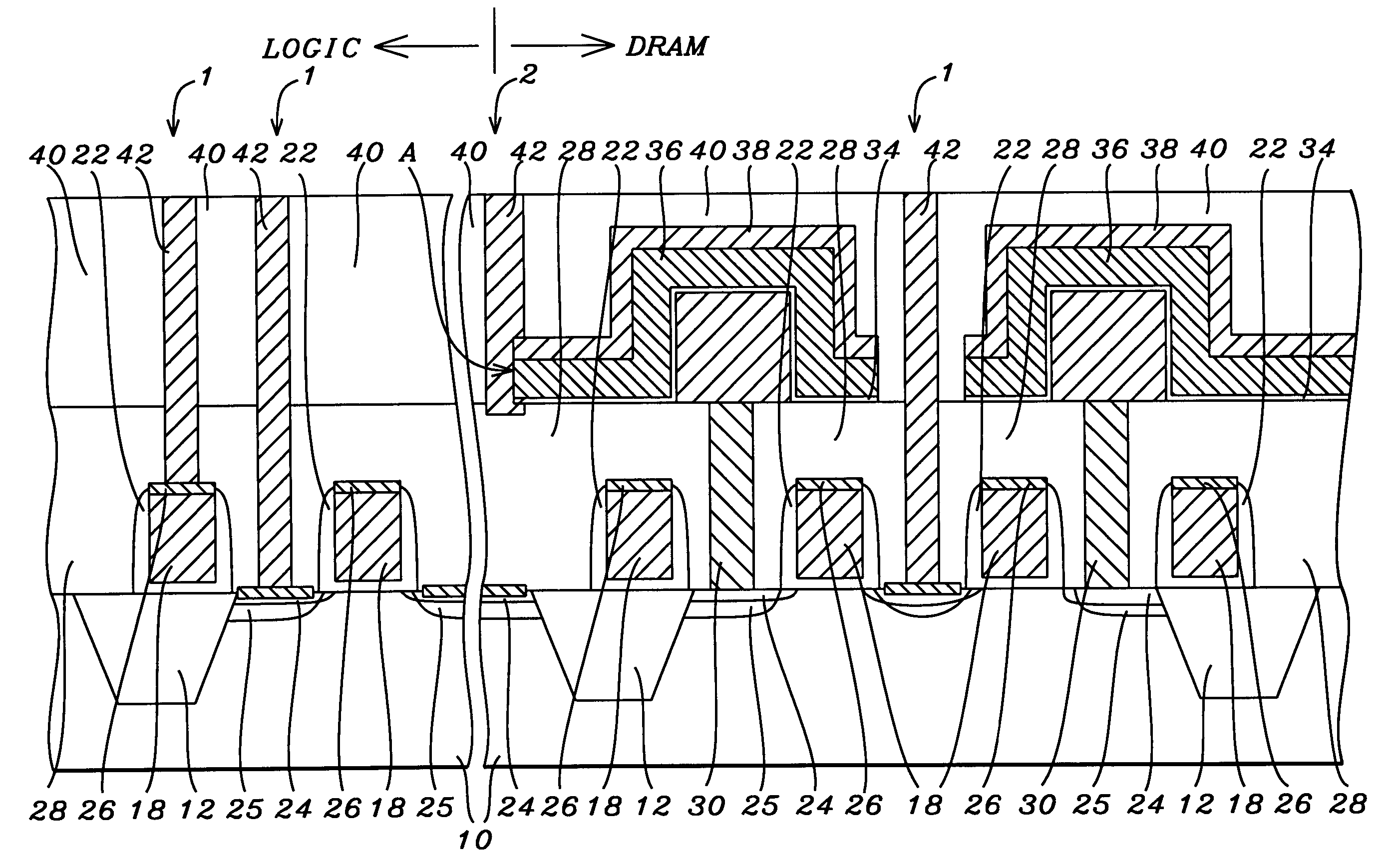
[0022] The method for making contact openings of varying depths in a planar insulating layer on a substrate having logic / memory circuits using a single masking and etching step is now described in detail. The method results in contacts that are damage-free at the substrate surface while providing contact openings for low-contact resistance to capacitor top electrodes with an anti-reflective coating (ARC). Although the invention is described for making contacts to top electrodes of a stacked or a trench capacitor, it should be understood by those skilled in the art that the contact openings can be made, in general, to a conducting layer having an ARC on the surface. However, the method is particularly useful for making low-resistance contacts to capacitor top electrodes.

[0023] Referring now to FIG. 3, the method begins by providing a semiconductor substrate 10, a portion of which is shown in the FIGS. FIG. 3 shows a schematic cross-sectional view of the substrate having a logic regi...


PUM


Abstract

A method for fabricating an insulating layer having contact openings of varying depths for logic/DRAM circuits is achieved using a single mask and etch step. After forming stacked or trench capacitors, a planar insulating layer is formed. Contact openings are etched in the planar insulating layer to the substrate, and contact openings that extend over the edge of the stacked or trench capacitor top electrode, having an ARC, are etched using a novel mask design and a single etching step. This allows one to make contacts to the substrate without overetching while making low-resistance contacts to the sidewall of the capacitor top electrode. In the trench capacitor open areas are formed to facilitate making contact openings that extend over the top electrode. A series of contact openings that are skewed or elongated also improve the latitude in alignment tolerance.

Description

BACKGROUND OF THE INVENTION [0001] (1) Field of the Invention [0002] This invention relates to semiconductor integrated circuit devices, and more particularly to a structure and method for making contact openings for embedded dynamic random access memory (DRAM) circuits. The structure and process are particularly useful for making contact openings in an insulating layer to the top electrode of the DRAM capacitor with low contact resistance, while concurrently etching contact openings to the substrate for bit-line contact openings and for contact openings to the logic areas without overetching the contact areas which would otherwise result in high leakage currents. [0003] (2) Description of the Prior Art [0004] Integrated logic and DRAM structures, also referred to as embedded memory, are becoming increasingly important for future product applications. These advanced circuits require field effect transistors (FETs) with shallower diffused junctions in logic areas to improve performan...

Claims


Application Information

Patent Timeline
Patent Type & Authority Applications(United States)
IPC IPC(8): H01L21/44H01L21/768H01L21/8242H01L23/48H01L27/108H01L29/40
CPCH01L21/76802H01L27/10811H01L27/10897H01L27/10894H01L27/10852H01L23/485H10B12/312H10B12/033H10B12/50H10B12/09
Inventor TU, KUO-CHI
Owner TAIWAN SEMICON MFG CO LTD
Why Eureka
Try Eureka