Microcomputer and microprocessor having flash memory operable from single external power supply

a microprocessor and flash memory technology, applied in static storage, digital storage, instruments, etc., can solve the problems of insufficient stability of programming and erasure of internal flash memory, and the simple effect of internal voltage boosting, so as to prevent non-volatile memory and minimize variations

Inactive Publication Date: 2005-05-05
RENESAS ELECTRONICS CORP
View PDF15 Cites 21 Cited by
  • Summary
  • Abstract
  • Description
  • Claims
  • Application Information

AI Technical Summary

Benefits of technology

[0022] Where the semiconductor integrated circuit device is programmed upon completion of a wafer (e.g., logical “0” of a low threshold voltage) and is erased upon shipment (e.g., logical “1” of a high threshold voltage), it is desirable to minimize variations that may occur in the output voltage of the voltage clamp means as a result of the voltages being extremely trimmed between the programming and the erasure states. The minimizing of such output voltage variations may be effected illustratively by the trimming control means including selective logic for determining trimming positions of the trimming circuit in accordance with the trimming adjustment information in such a manner that the trimming position in effect when the trimming adjustment information has an all-bit logic value of “1” is adjacent to the trimming position in effect when the trimming adjustment information has an all-bit logic value of “0”. In this setup, the voltage output by the voltage clamp means may be minimized in terms of difference between where the non-volatile memory is programmed upon completion of a wafer, and where the non-volatile memory is erased upon shipment.
[0023] It takes some time for the boosting means to gain a required boosted voltage. The required time is known to suffer from process-dependent variations. A programming and an erasure operation must each be started after the boosted voltage has reached a predetermined voltage level. These aspects are controlled by the central processing unit running suitable software. Illustratively, the inventive semiconductor integrated circuit device may comprise a control register for controlling the non-volatile memory, the control register including: a programming set-up bit for instructing the boosting means to start a boosting operation for programming; a programming enable bit for designating a start of a programming operation by use of the boosted voltage; an erasing set-up bit for instructing the boosting means to start a boosting operation for erasure; and an erasing enable bit for designating a start of an erasing operation by use of the boosted voltage. This arrangement eliminates the need for additionally providing hardware, such as a timer, for controlling when to start the actual erasing or programming the device after the erasure or the programming has been designated.
[0024] Furthermore, the control register may include a programming of enable bit for instructing the boosting means to prepare for a boosting operation, so that the instruction based on any of the erasing set-up bit and the programming set-up bit is accepted only if the programming enable bit is set to its true value. That is, a programming or erasure operation is carried out on condition that the programming enable bit be set to the true value. This arrangement helps prevent the non-volatile memory from getting inadvertently reprogrammed, for example, by a runaway central processing unit.

Problems solved by technology

The inventors have found that the channel that the channel injection method was not suitable for internal voltage boosting because of its need for a relatively large current.
With the tunnel current method, on the other hand, simply effecting internal voltage boosting was found insufficient to implement programming and erasure of an internal flash memory in a stable manner within a relatively wide range of external power supply voltages, including those for low-voltage operations.

Method used


Image

  • Microcomputer and microprocessor having flash memory operable from single external power supply
  • Microcomputer and microprocessor having flash memory operable from single external power supply
  • Microcomputer and microprocessor having flash memory operable from single external power supply

Examples


Embodiment Construction

Microcomputer Chip

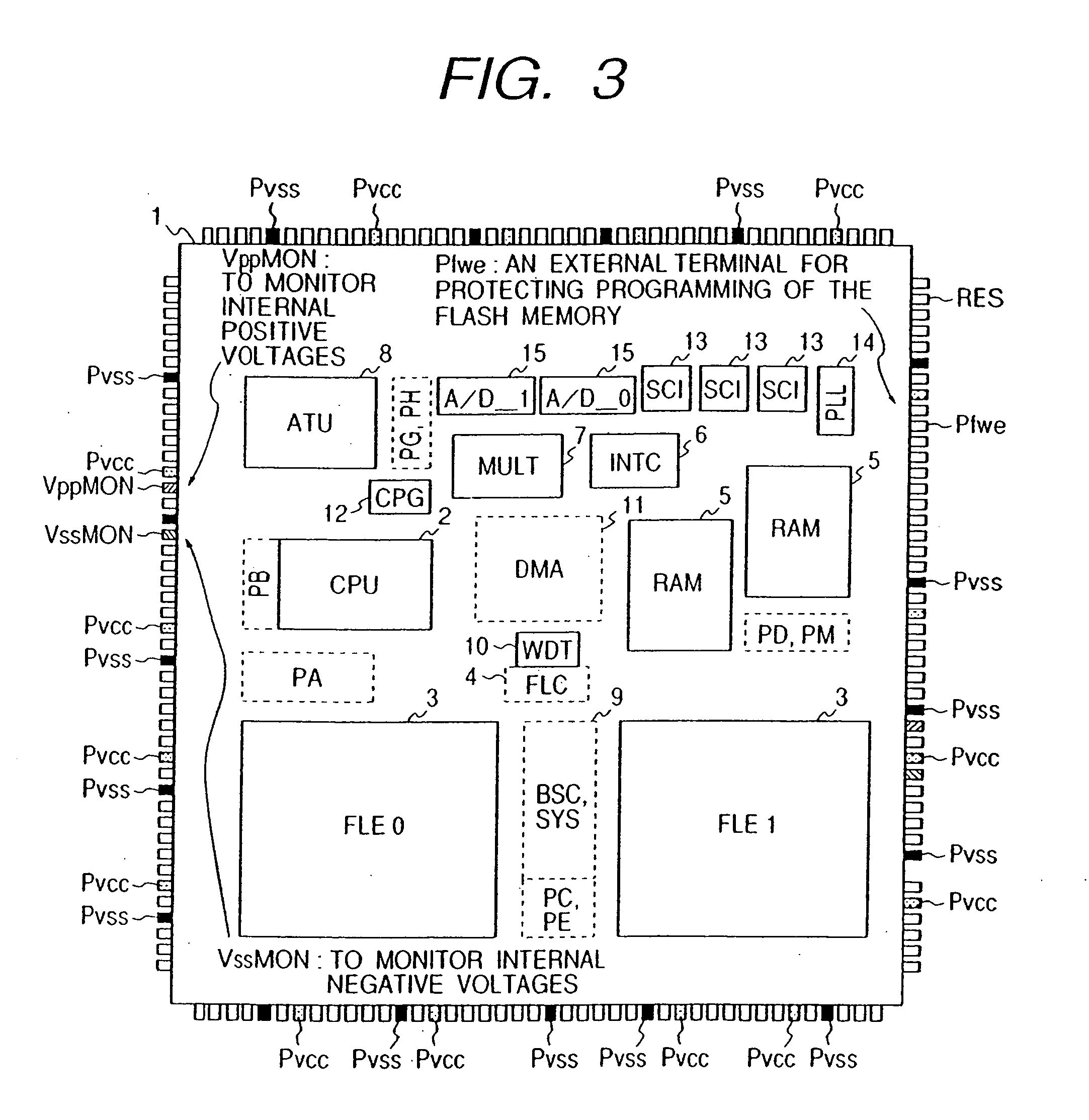
[0059]FIG. 3 is a block diagram of a microcomputer 1 (microprocessor or data processor) according to the invention The microcomputer 1 is formed by use of well-known semiconductor integrated circuit fabrication techniques illustratively on a single semiconductor substrate made of materials such as single crystal silicon.

[0060] The microcomputer 1 in FIG. 3 comprises, but the invention is not limited to, a central processing unit (CPU) 2, flash memories (FLE0, FLE1) 3, a flash memory control register (FLC) 4, random access memories (RAM) 5, an interrupt controller (INTC) 6, a multiplier (MULT) 7, a timer (ATU) 8, a bus and a system controller (BSC, SYS) 9, a watch dog timer (WDT) 10, a direct memory access controller (DMA) 11, a clock pulse generator (CPG) 12, serial communication interfaces (SCI) 13, a phase locked loop circuit (PLL) 14, analog-to-digital converters (A / D0, A / D—1), and a plurality of I / O ports PA, PB, PC, PD, PE, PG, PH and PM. The circuit blocks...


PUM


Abstract

A microcomputer incorporating a flash memory which is erased and programmed electrically in a stable manner within a relatively wide range of external power supply voltages including those for low-voltage operations The microcomputer comprises a voltage-clamp unit including a reference voltage generating circuit and a constant voltage generating circuit. In operation, the voltage clamp unit generates a voltage of a low dependency on a supply voltage and clamps the generated voltage to a voltage level which, within a tolerable range, is lower than a single supply voltage externally furnished. This prevents voltages boosted by boosting circuits operating on the clamped voltage, i.e., programming and erasure voltages, from being dependent on the externally supplied voltage.

Description

BACKGROUND OF THE INVENTION [0001] The present invention relates to a semiconductor integrated circuit device comprising a non-volatile memory and a central processing unit More particularly, the invention relates to techniques for providing a single-chip microcomputer, a data processing device, or a microprocessor which includes a flash memory and a central processing unit having a single external power supply. [0002] Microcomputers incorporating a flash memory are known by the designations H8 / 538F, H8 / 3048 and H8 / 3434F, available from Hitachi, Ltd. [0003] Memory cell transistors constituting a flash memory each have a floating gate, a control gate, a source and a drain. As such, each memory cell transistor retains binary information representing a charge injection state of its floating gate For example, electrically charging the floating gate of a memory cell transistor brings a threshold voltage of that memory cell into a high state. When the threshold voltage is raised relative ...

Claims


Application Information

Patent Timeline
Patent Type & Authority Applications(United States)
IPC IPC(8): G11C5/14G11C16/30
CPCG11C5/14G11C5/145G11C16/30G11C16/12G11C5/147
Inventor ISHIKAWA, EIICHISAITO, YASUYUKISATO, MASANAOYADA, NAOKIMATSUBARA, KIYOSHI
Owner RENESAS ELECTRONICS CORP
Why Eureka
Try Eureka