Non-volatile memory and method of manufacturing floating gate

a floating gate, non-volatile technology, applied in the direction of semiconductor devices, electrical equipment, nanotechnology, etc., can solve the problems of difficult to obtain desirable lower operating voltage, easy to occur electrical leakage, and affect device reliability, etc., to achieve the effect of improving the reliability of memory devices

Inactive Publication Date: 2005-05-05
NAT SUN YAT SEN UNIV
View PDF4 Cites 51 Cited by
  • Summary
  • Abstract
  • Description
  • Claims
  • Application Information

AI Technical Summary

Benefits of technology

[0008] In view of the above, the present invention is directed to a method of manufacturing a floating gate, which can be employed to enhance reliability of memory devices.
[0012] In this invention, since the nano-dots or film containing a semiconductor component is used as an charge storing unit, when defects exist in the tunneling layer, only the charge of the nano-dots or film near the defective portion will be lost while the charge in other portions remains, so that the reliability of the device can be enhanced. In addition, even if the thickness of the tunneling layer is reduced, the reliability of the device will not be reduced, and thus the operating voltage can be lowered and the speed of write / erase operation can be increased.

Problems solved by technology

Upon multiple operations, if defects exist in the tunneling oxide layer below the layer of the polysilicon floating gate, electric leakage may easily occur to affect the device reliability.
As a result, the thickness of the tunneling oxide layer cannot be reduced and a desirable lower operating voltage is hard to be obtained.

Method used


Image

  • Non-volatile memory and method of manufacturing floating gate
  • Non-volatile memory and method of manufacturing floating gate
  • Non-volatile memory and method of manufacturing floating gate

Examples


first embodiment

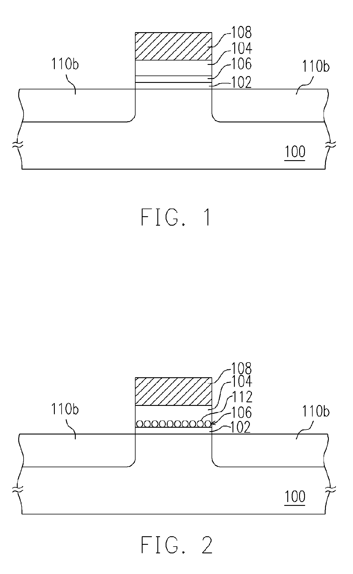
[0039] First Embodiment

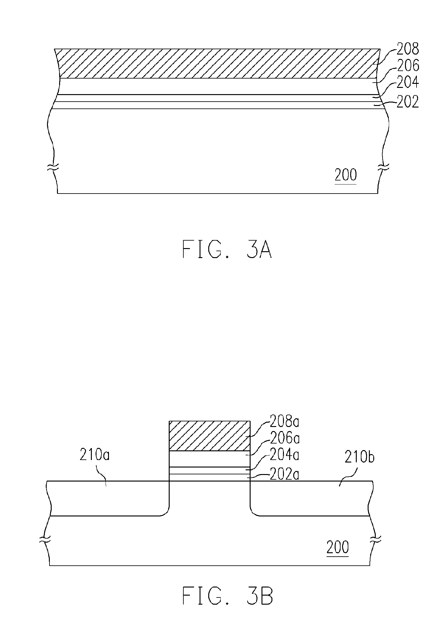
[0040] A first preferred embodiment of method of manufacturing the non-volatile memory of this invention is illustrated in FIGS. 3A and 3B.

[0041] Referring to FIG. 3A, a tunneling layer 202 is formed on a substrate 200. The substrate 200 is a silicon substrate for example, while the tunneling layer 202 is made of silicon oxide or other kind of dielectric, and is formed via a process such as thermal oxidation or chemical vapor deposition. In this embodiment, the tunneling layer 202 of silicon oxide is formed, for example, via dry oxidative deposition of a film of about 5 nm in a chemical vapor deposition chamber at 925° C. under normal pressure.

[0042] A semiconductor oxide layer 204 is then formed on the tunneling layer 202. The semiconductor oxide layer 204 is a film used as a floating gate. Here, the semiconductor oxide refers to element semiconductor or compound semiconductor. The semiconductor oxide layer 204 contains semiconductor components, which inclu...

second embodiment

[0046] Second Embodiment

[0047] A second preferred embodiment of method of manufacturing the non-volatile memory of this invention is illustrated in FIGS. 5A to 5D.

[0048] Referring first to FIG. 5A, a substrate 200 is provided and a tunneling layer 202 is formed thereon. A semiconductor silicide layer 400 is then formed on the tunneling layer 202, wherein the semiconductor silicide refers to silicide of element semiconductor or compound semiconductor. The semiconductor silicide layer 400 contains semiconductor components, for example, as described in the first preferred embodiment. The semiconductor silicide layer 400, when made of Si1-xGex (0400 is formed via a process of, for example, low-pressure chemical vapor deposition, while a layer of Si1-xGex in a thickness of, for example, 20 nm is formed on the tunneling layer 202. The low-pressure chemical vapor deposition is carried out at about 550° C. and under about 460 mTorr, while the process gases are SiH4 and GeH4.

[0049] Referri...

third embodiment

[0054] Third Embodiment

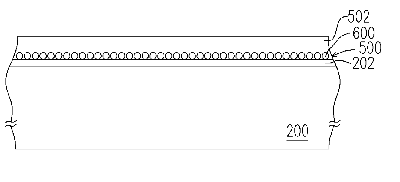
[0055] A third preferred embodiment of method of manufacturing the non-volatile memory of this invention is illustrated in FIGS. 6A to 6C.

[0056] Referring first to FIG. 6A, a substrate 200 is provided, and a tunneling layer 202 is formed thereon. A semiconductor layer 500, a thin film, is then formed on the tunneling layer 202, while the semiconductor layer 500 is made of, for example, the components as mentioned in the first embodiment. In this embodiment, the semiconductor layer 500 is made of, for example, germanium (Ge) in a thickness of 1 to 10 nm, and is formed, for example, via a process of physical vapor deposition or chemical vapor deposition. The process is carried out at a temperature of, for example, between 100 to 1000° C., and under a pressure of, for example, between 1 to 500 mTorr. The process of chemical vapor deposition can be, for example, low-pressure chemical vapor deposition, plasma enhanced chemical vapor deposition, high-density plasma...


PUM


Abstract

A method of manufacturing a floating gate is provided. The method includes the steps of forming a tunneling layer on a substrate, and forming a film layer containing a semiconductor component on the tunneling layer. The film layer consists of a semiconductor film or nano-dots.

Description

CROSS-REFERENCE TO RELATED APPLICATION [0001] This application claims the priority benefit of Taiwan application serial no. 92130674, filed Nov. 3, 2003 and Taiwan application serial no. 93118989, filed Jun. 29, 2004. BACKGROUND OF THE INVENTION [0002] 1. Field of the Invention [0003] The present invention relates to a memory device, and more particularly to a non-volatile memory and a method of manufacturing a floating gate. [0004] 2. Description of the Related Art [0005] Electronically erasable and programmable read only memory (EEPROM), among various of non-volatile memory devices, is suitable of performing multiple operations of writing, read and erasure, and is non-volatile even when power is off. As a result, EEPROM becomes a type of memory device widely used in personal computers and other electronic equipments. [0006] In a EEPROM, doped polysilicon is conventionally used for fabricating a floating gate and a control gate. A dielectric layer is used to separate the floating g...

Claims


Application Information

Patent Timeline
Patent Type & Authority Applications(United States)
IPC IPC(8): H01L21/28H01L21/336H01L29/423
CPCB82Y10/00H01L21/28273H01L29/7881H01L29/66825H01L29/42332H01L29/40114
Inventor CHANG, TING-CHANGYAN, SHUO-TINGLIU, PO-TSUNCHEN, CHI-WENTSAI, TSUNG-MINGTAI, YA-HSIANGSZE, SIMON-M
Owner NAT SUN YAT SEN UNIV
Why Eureka
Try Eureka