Interconnection for chip sandwich arrangements, and method for the production thereof

a technology of interconnection and sandwich structure, which is applied in the direction of contact member manufacturing, basic electric elements, solid-state devices, etc., can solve the problems of unsuitability of wire bonding technology for 3-d chip systems, and high loss of wires, so as to achieve low-outlay production

Inactive Publication Date: 2005-05-12
POLARIS INNOVATIONS LTD
View PDF10 Cites 3 Cited by
  • Summary
  • Abstract
  • Description
  • Claims
  • Application Information

AI Technical Summary

Benefits of technology

[0016] A particular feature of the invention is to be seen in the fact that the contact elements may be arranged perpendicularly or else without any problems obliquely between the chips. This makes it possible to compensate for slight positional deviations of the contacts that are to be connected to one another.
[0018] This method for producing the contact elements can be realized extremely cost-effectively without any photolithography.
[0025] In a further advantageous development, the flexible substrate is a flexible printed circuit board whose conductive tracks (e.g., copper tracks) are contact-connected during the metalization of the microvias. This makes it possible, in a simple manner, to achieve a rewiring of the chip contacts and also to realize a connection to peripheral devices.
[0026] One particular advantage of the contact elements according to a preferred embodiment of the invention is to be seen in the fact that they can be produced with low outlay and with conventional technology, and that it is possible to dispense with the chemical deposition of copper, which may be replaced by means of an electrolytic direct metalization. The vias may be produced simultaneously simply by plasma etching.

Problems solved by technology

These customary wirings have the disadvantage of high losses and are therefore extremely unsuitable for chips of the new generation having high clock frequencies.
Furthermore, the wire bonding technology is technologically unsuitable for 3-D chip systems because the outlay for producing the wire bridges is considerable and the risk of short circuits between the wire bridges rises as the contact density increases.
In the meantime, chip sandwich structures have become known in which chips are stacked face-to-face, the production of the direct connections between the chips being relatively complicated.
However, the outlay for realizing these interconnections is considerable owing to the required photolithography.

Method used


Image

  • Interconnection for chip sandwich arrangements, and method for the production thereof
  • Interconnection for chip sandwich arrangements, and method for the production thereof

Examples


Embodiment Construction

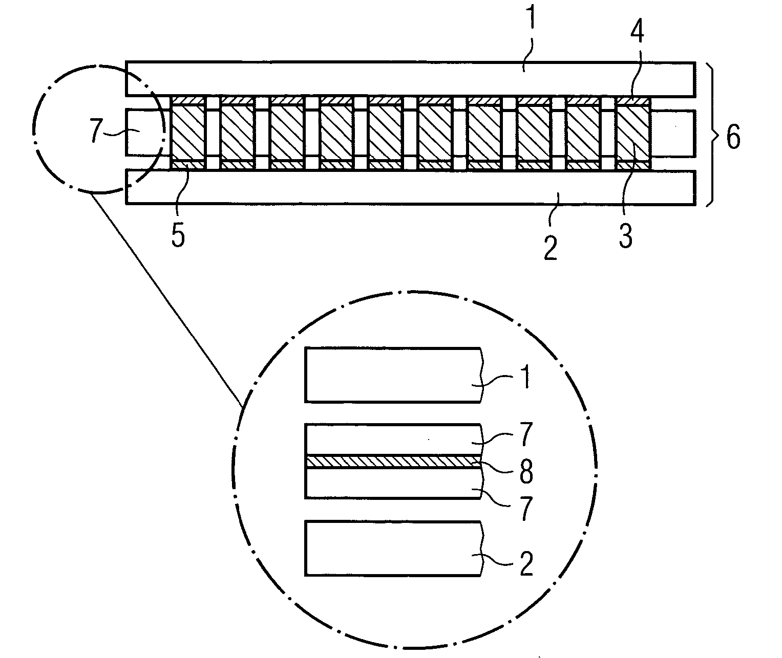
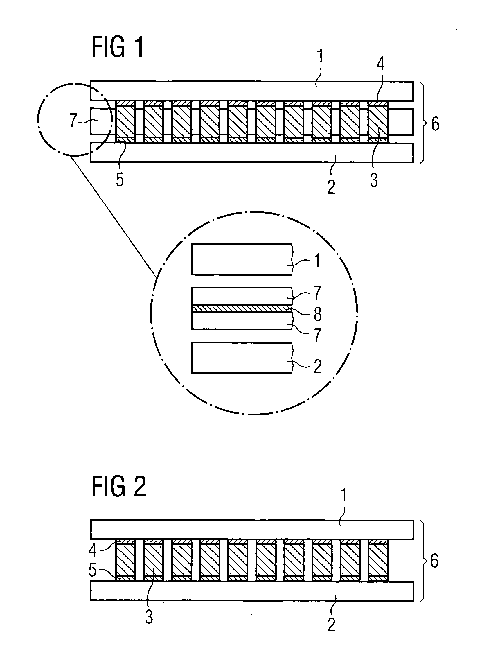
[0030]FIG. 1 illustrates an interconnection according to a preferred embodiment of the invention between two chips 1, 2 in a face-to-face arrangement. These chips 1, 2 are connected to one another by means of pin- or sleeve-shaped contact elements 3. For this purpose, the contact elements 3 are soldered to contact pads 4, 5 on the chips 1, 2, thereby creating an electrical and mechanical interconnection in the contact pads 4, 5 of the chips.

[0031] The pin- or sleeve-shaped contact elements 3 preferably ensure a shortest possible connection between the chips 1, 2 and at the same time enable a mechanically fixed composite to form a chip sandwich 6.

[0032] In order to simplify the mounting, the contact elements 3 are embedded in a flexible substrate 7, which may comprise a flexible polymer substrate, for example. In this case, the contact elements 3 are arranged in the pitch of the contact pads 4, 5 in a manner similar to an FBGA structure of the chips that are to be contact-connected...


PUM

PropertyMeasurementUnit
thicknessaaaaaaaaaa
clock frequenciesaaaaaaaaaa
flexibleaaaaaaaaaa

Abstract

The invention relates to an interconnection for chip sandwich structures by means of which chips can be electrically and mechanically connected to one another face-to-face, and to a method for the production thereof. The invention is intended to create interconnections that can be produced more cost-effectively and more effectively. This is achieved by virtue of the fact that pin- or sleeve-shaped contact elements (3) are arranged between the chips (1, 2), which contact elements create an electrical and mechanical interconnection between the contact pads (4, 5) of the semiconductor chips (1, 2) and are soldered to the latter.

Description

[0001] This application claims priority to German Patent Application 103 43 257.4, which was filed Sep. 17, 2003, and is incorporated herein by reference. TECHNICAL FIELD [0002] The invention relates to an interconnection for chip sandwich structures, by means of which chips can be electrically and mechanically connected to one another face-to-face, and to a method for the production thereof. BACKGROUND [0003] It has been found that the demands for compact handheld products such as miniature PCs, portable navigation systems, databases, telephones etc. is constantly continually rising. These products require particularly small memories with a high storage capacity and must realize rising switching frequencies and power densities without any problems. In order to be able to meet these requirements, recently use has been made of so-called “chip sandwich constructions.”[0004] In the case of such chip sandwich constructions, chips at the wafer level are stacked to form a 3-D chip system ...

Claims


Application Information

Patent Timeline
Patent Type & Authority Applications(United States)
IPC IPC(8): H01L23/498H01L25/065
CPCH01L23/49827H01L25/0657Y10T29/49204H01L2225/06572H01L2924/0102H01L2224/16H01L2224/05573H01L2224/05568H01L2924/00014H01L2224/05599
Inventor HANKE, ANDRE
Owner POLARIS INNOVATIONS LTD
Why Eureka
Try Eureka