Method of manufacturing a reflection type mask blank and method of manufacturing a reflection type mask

Inactive Publication Date: 2005-05-12
HOYA CORP
View PDF3 Cites 23 Cited by
  • Summary
  • Abstract
  • Description
  • Claims
  • Application Information

AI Technical Summary

Benefits of technology

[0022] The stress correction film is preferably made of an amorphous material comprising metal or alloy. Such material provides a film excellent in smoothness and facilitates adjustment of the value of the initial stress to be given to the stress correction film.
[0023] Moreover, a reflection type mask can be produced by forming a pattern on the absorber layer of

Problems solved by technology

As a consequence, the multilayer reflection film inevitably has a high compression stress.
If the compression stress of the multilayer film is large as described above, the warp of the surface of the multilayer reflection film causes the decrease in transfer accuracy (image placement error) during transfer to the wafer.
This results in a problem that high-accuracy transfer is impossib

Method used


Image

  • Method of manufacturing a reflection type mask blank and method of manufacturing a reflection type mask
  • Method of manufacturing a reflection type mask blank and method of manufacturing a reflection type mask
  • Method of manufacturing a reflection type mask blank and method of manufacturing a reflection type mask

Examples


examples)

(EXAMPLES)

[0094] Next, this invention will be explained more in detail in conjunction with examples of this invention.

example 1

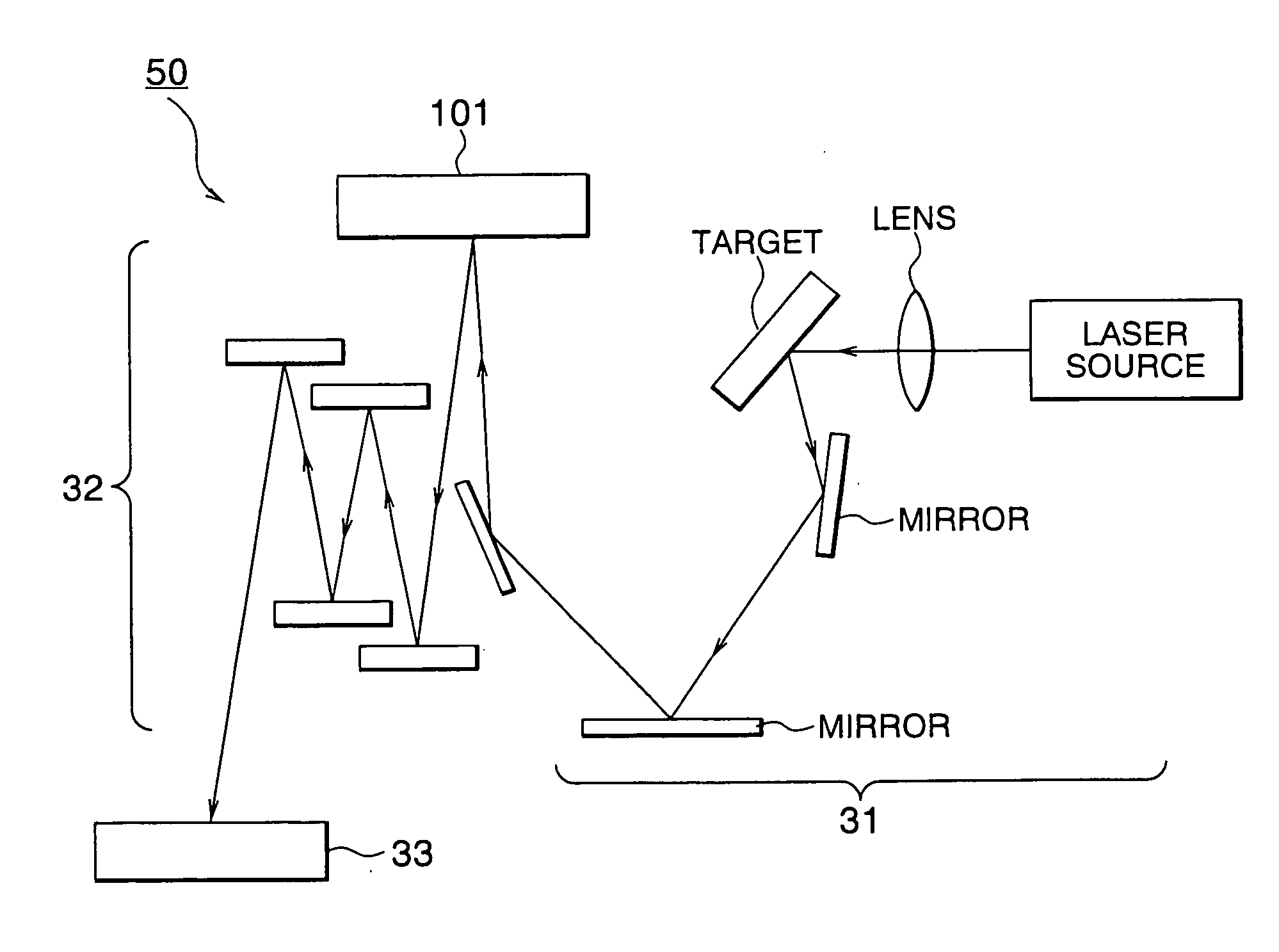
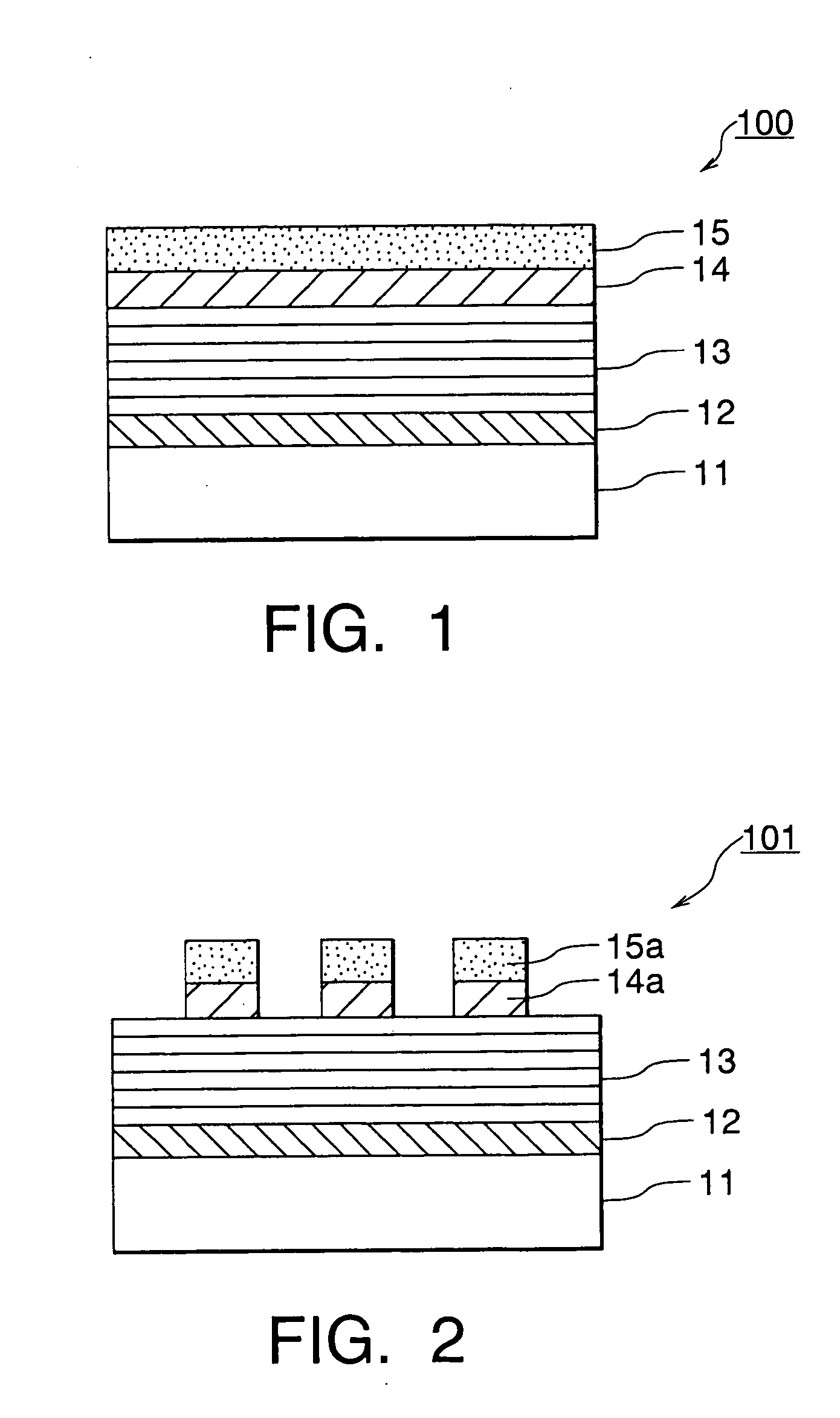
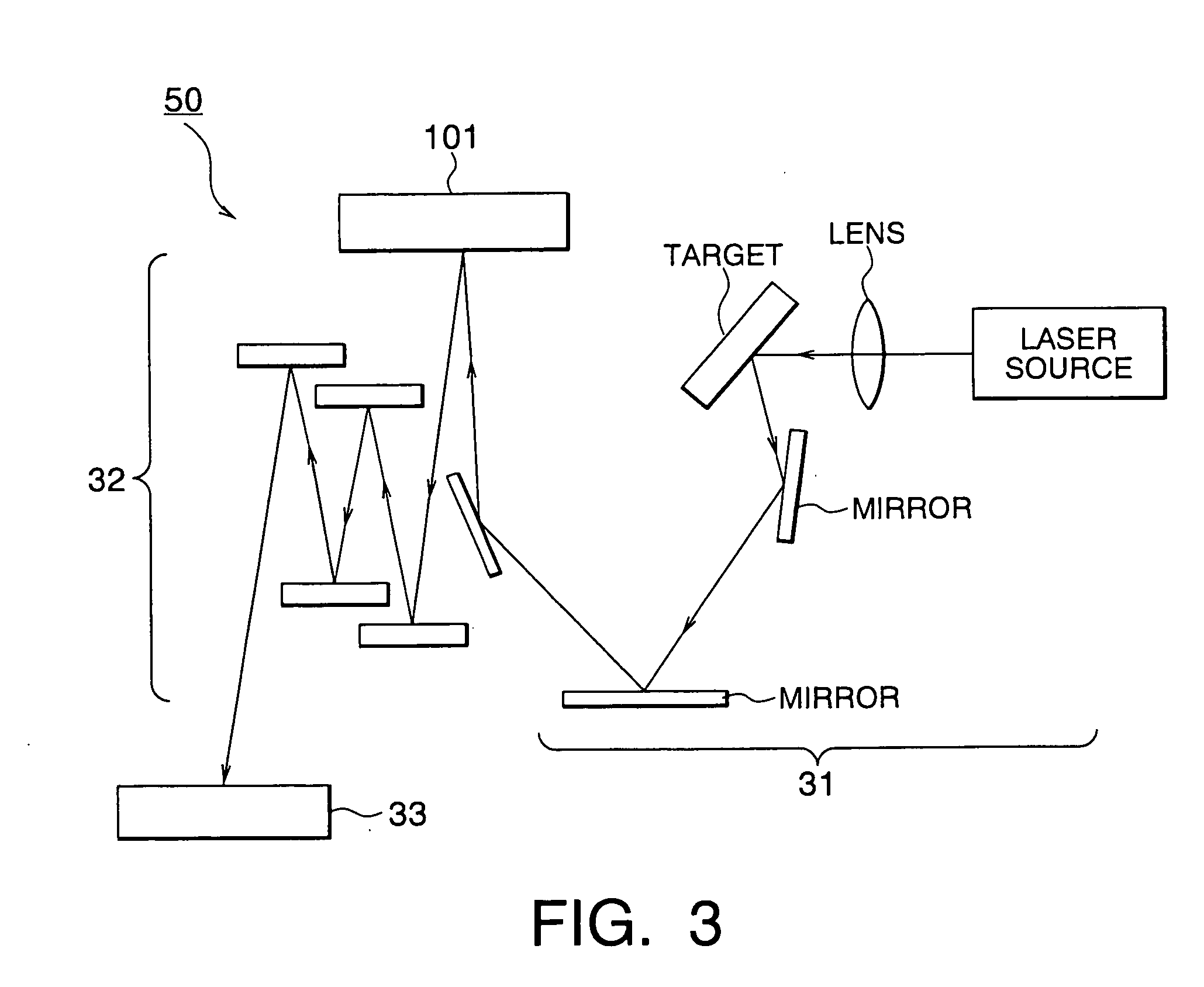
[0095] Referring to FIG. 1 and FIG. 2, description will be made of a method of manufacturing an EUV reflection type mask blank 100 and an EUV reflection type mask 101 according to this example. FIG. 1 is a sectional view of the reflection type mask blank while FIG. 2 is a sectional view of the reflection type mask.

[0096] A substrate 11 was a SiO2—TiO2 based glass substrate (outer dimension of 6 inch square, thickness of 6.3 mm). The substrate 11 had a coefficient of thermal expansion of 0.2×10⁻⁷ / ° C. and Young's modulus of 67 GPa. The glass substrate was subjected to mechanical polishing to have a smooth surface of 0.2 nmRms or less and a flatness of 100 nm or less.

[0097] At first, on the substrate 11, a film containing Ta and B was deposited to a thickness of 70 nm as a stress correction film 12. The deposition was carried out using a target containing Ta and B by the DC magnetron sputtering using Ar gas. At this time, by controlling the sputtering condition, the stress of the st...

example 2

[0116] In this example, the reflection type mask blank was formed in the manner similar to Example 1 except that the condition upon deposition of the stress correction film 12 was changed and the film stress initially given to the stress correction film was +50 MPa and that the heat treatment condition was set at 200° C. for 60 minutes.

[0117] The following Table 2 collectively shows the film thickness, the surface roughness, the stress before and after the heat treatment, and the flatness for each of the stress correction film and the multilayer reflection film. In this example, the stress of the substrate with the multilayer reflection film as a whole was sufficiently lowered to +66 MPa (the value scaled to the film thickness equivalent to that of the multilayer film) by the heat treatment. The

TABLE 2Example 1 (Heating Condition 200° C., 60 min)Before HeatingAfter HeatingFilmSurfaceStress × FilmStress × FilmThicknessRoughnessStressThicknessFlatnessStressThicknessFlatnessMaterial...


PUM

PropertyMeasurementUnit
Temperatureaaaaaaaaaa
Pressureaaaaaaaaaa
Pressureaaaaaaaaaa

Abstract

A method of manufacturing a reflection type mask blank by forming a multilayer reflection film reflecting exposure light on a substrate and forming an absorber layer absorbing the exposure light on the multilayer reflection film includes a step of forming, between the substrate and the multilayer reflection film, a stress correction film opposite in direction to film stress of the multilayer reflection film and smaller in absolute value than the film stress of the multilayer reflection film, a step of heat-treating the stress correction film, and a step of heat-treating the multilayer reflection film.

Description

[0001] This application claims priority to prior Japanese application JP 2002-242923, the disclosure of which is incorporated herein by reference. BACKGROUND OF THE INVENTION [0002] This invention relates to a method of manufacturing a reflection type mask blank for exposure for use in a pattern transfer of a semiconductor device and a method of manufacturing a reflection type mask. [0003] In a recent semiconductor industry, with miniaturization of a semiconductor device, EUV lithography as an exposure technique using Extreme Ultra Violet light (will hereinafter be abbreviated to EUV light) is promising. It is noted here that the EUV light means light having a wavelength band within a soft X-ray region or a vacuum ultraviolet ray region, more specifically, light having a wavelength of about 0.2-100 nm. As a mask used in the EUV lithography, a reflection type mask for exposure is proposed, for example, as disclosed in Japanese Unexamined Patent Publication No. 8-213303. [0004] Such a...

Claims


Application Information

Patent Timeline
IPC IPC(8): B32B9/00B32B17/06C03C17/34G03C5/00G03F1/14G03F9/00
CPCB82Y10/00G03F1/24C03C17/3482B82Y40/00
Inventor SHOKI, TSUTOMUHOSOYA, MORIOKINOSHITA, TAKERU
Owner HOYA CORP
Why Eureka
Try Eureka