Large area, uniformly low dislocation density GaN substrate and process for making the same
a gallium nitride and large area technology, applied in the direction of natural mineral layered products, instruments, transportation and packaging, etc., can solve the problems of large area gan substrates, large gan substrates, and low-cost manufacturing of gan-based devices
- Summary
- Abstract
- Description
- Claims
- Application Information
AI Technical Summary
Benefits of technology
Problems solved by technology
Method used
Image

Examples
example 1
Single Wafer Process
[0108] In this example, two-step GaN HVPE growth on a sapphire substrate was carried out. In the first stage of the growth, the growth temperature was 1010° C., the NH3 / HCl ratio was 17, the growth rate was about 160 μm / hr, and the thickness of the grown film was about 320 μm.
[0109] After the completion of the first step, the growth temperature was raised to 1030° C., and the NH3 / HCl ratio was reduced to 8.6, and growth was continued until the thickness of the second stage GaN material was about 640 μm.
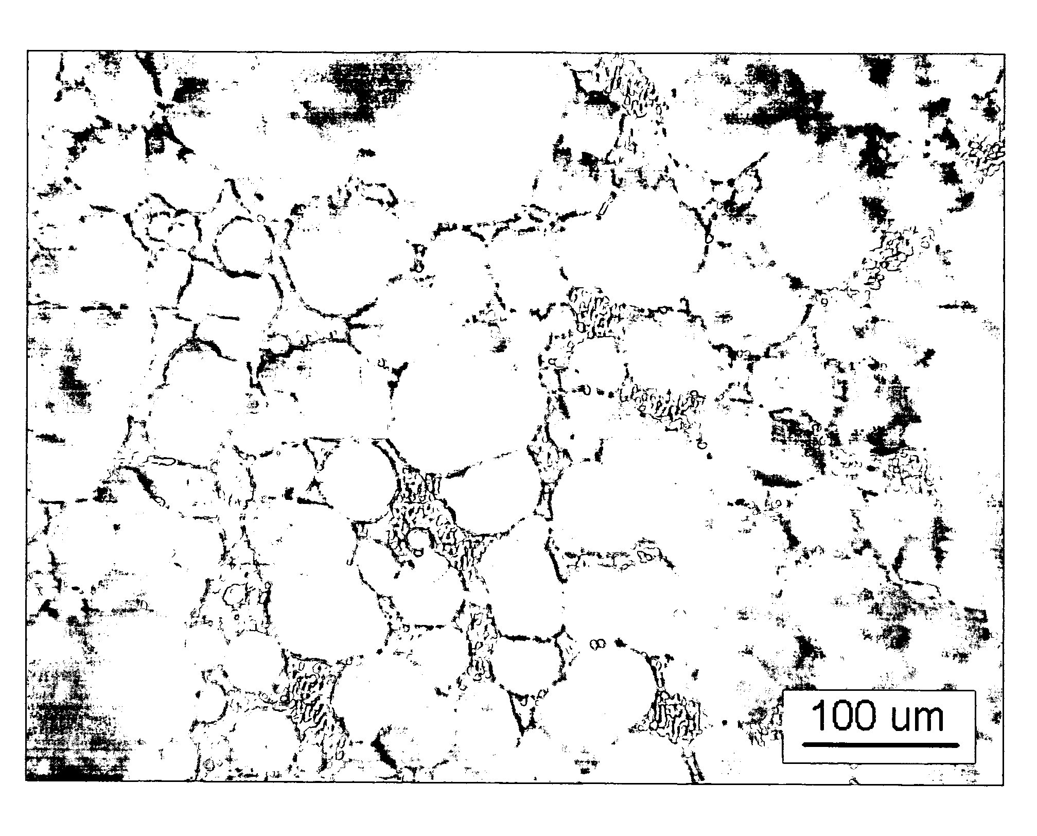
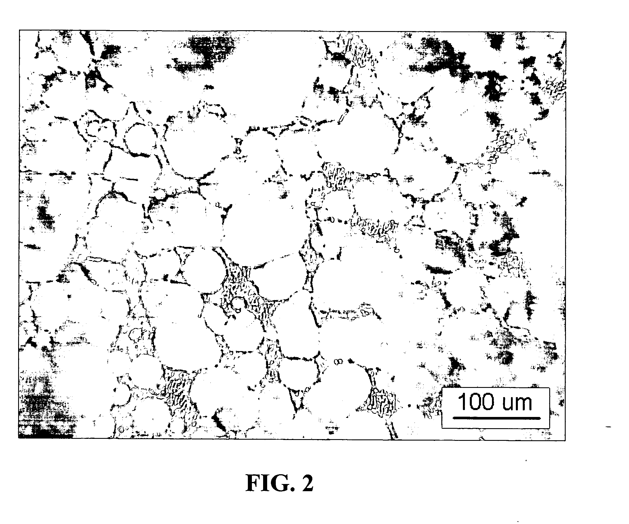
[0110] After the completion of the growth, the sapphire substrate was removed from the thick GaN film. The GaN wafer blank was first ground about its edge by mechanical means. The GaN wafer had two surfaces. The surface constituting the growth surface was gallium-terminated. The side that was attached to the sapphire substrate was the nitrogen-terminated side. The gallium-side of the wafer was first lapped with coarse diamond slurry on a lap machine, and then p...
example 2
GaN Ingot Process
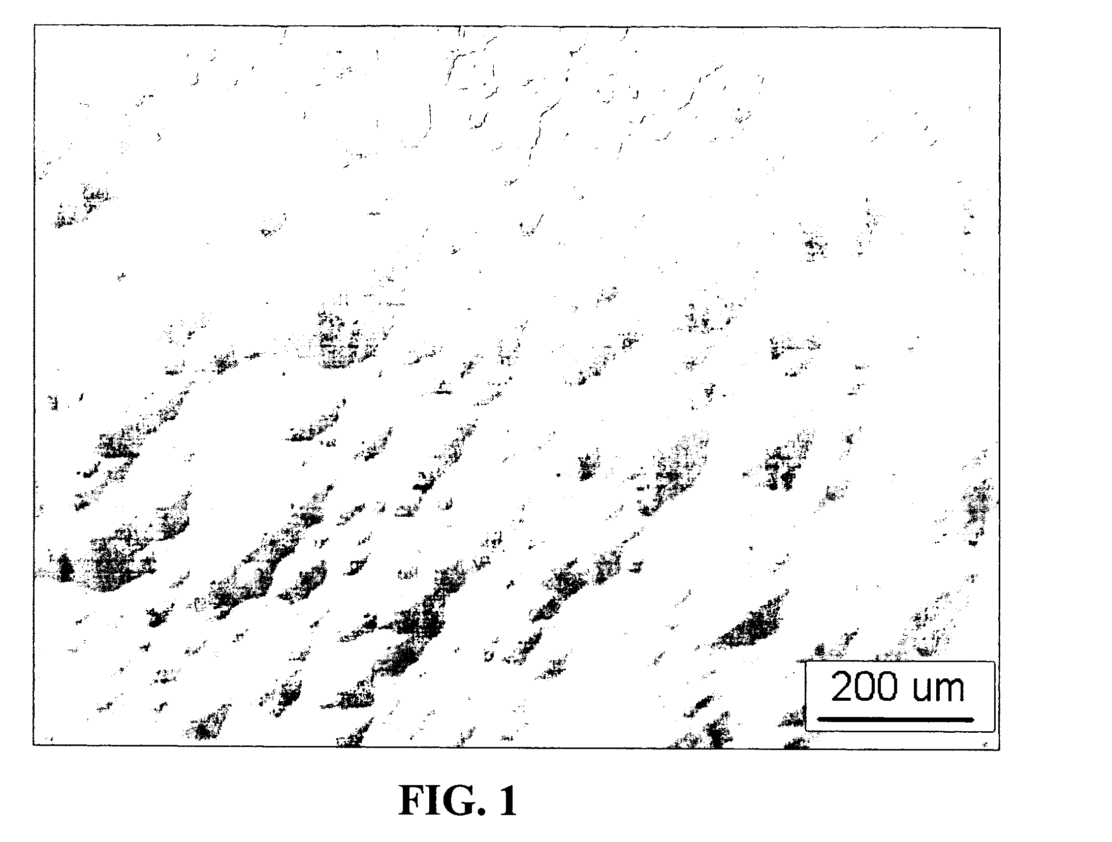
[0115] In this example, the two-step HVPE GaN growth process was carried out to grow a relatively long GaN ingot.
[0116] In the first stage of the growth process, the growth temperature was 1010° C., the NH3 / HCl ratio was 17, the growth rate was about 160 μm / hr, and the thickness of the grown film was about 320 μm.
[0117] After completion of the first step, the growth temperature was raised to 1030° C., and the NH3 / HCl ratio was reduced to 12.9. Growth of the GaN material was continued until the length of the ingot was 3.2 mm.
[0118] The ingot after its formation was processed into multiple wafers by slicing and subsequent lap, polish and chemical mechanical polish steps as in Example 1. Similar two-step HVPE GaN growth processes were carried out to grow GaN ingots having lengths on the order of 10 mm.
PUM
| Property | Measurement | Unit |
|---|---|---|
| Temperature | aaaaa | aaaaa |
| Fraction | aaaaa | aaaaa |
| Fraction | aaaaa | aaaaa |
Abstract
Description
Claims
Application Information
 - Generate Ideas
- Intellectual Property
- Life Sciences
- Materials
- Tech Scout
- Unparalleled Data Quality
- Higher Quality Content
- 60% Fewer Hallucinations
Browse by: Latest US Patents, China's latest patents, Technical Efficacy Thesaurus, Application Domain, Technology Topic, Popular Technical Reports.
© 2025 PatSnap. All rights reserved.Legal|Privacy policy|Modern Slavery Act Transparency Statement|Sitemap|About US| Contact US: help@patsnap.com