Plasma display panel

a technology of display panels and plasma, applied in static indicating devices, instruments, gas-filled discharge tubes, etc., can solve the problems of unstable address operation, difficult to secure brightness when higher definition is achieved, and too much time spent on address periods, etc., to reduce discharge voltage, reduce influence on surroundings, and form stably

Inactive Publication Date: 2005-05-19
PANASONIC CORP
View PDF10 Cites 9 Cited by
  • Summary
  • Abstract
  • Description
  • Claims
  • Application Information

AI Technical Summary

Benefits of technology

[0011] In this structure, at the time of a priming discharge performed by making the electrodes provided on the second substrate side function as cathodes, providing a material layer containing at least one of alkali metal oxide, alkaline earth metal oxide and fluoride can largely reduce a discharge voltage in priming discharge, and can

Problems solved by technology

In this type of PDP, a large delay in discharge occurs during the address period, thereby making the address operation unstable, or completion of the address operation requires a long address time, thereby spending too much time for the address period.
However, in these conventional PDPs, when the number of lines is increased as a result of achieved higher definition, more time must be spent for the address time and less ti

Method used


Image

  • Plasma display panel
  • Plasma display panel
  • Plasma display panel

Examples


first exemplary embodiments

(First Exemplary Embodiments)

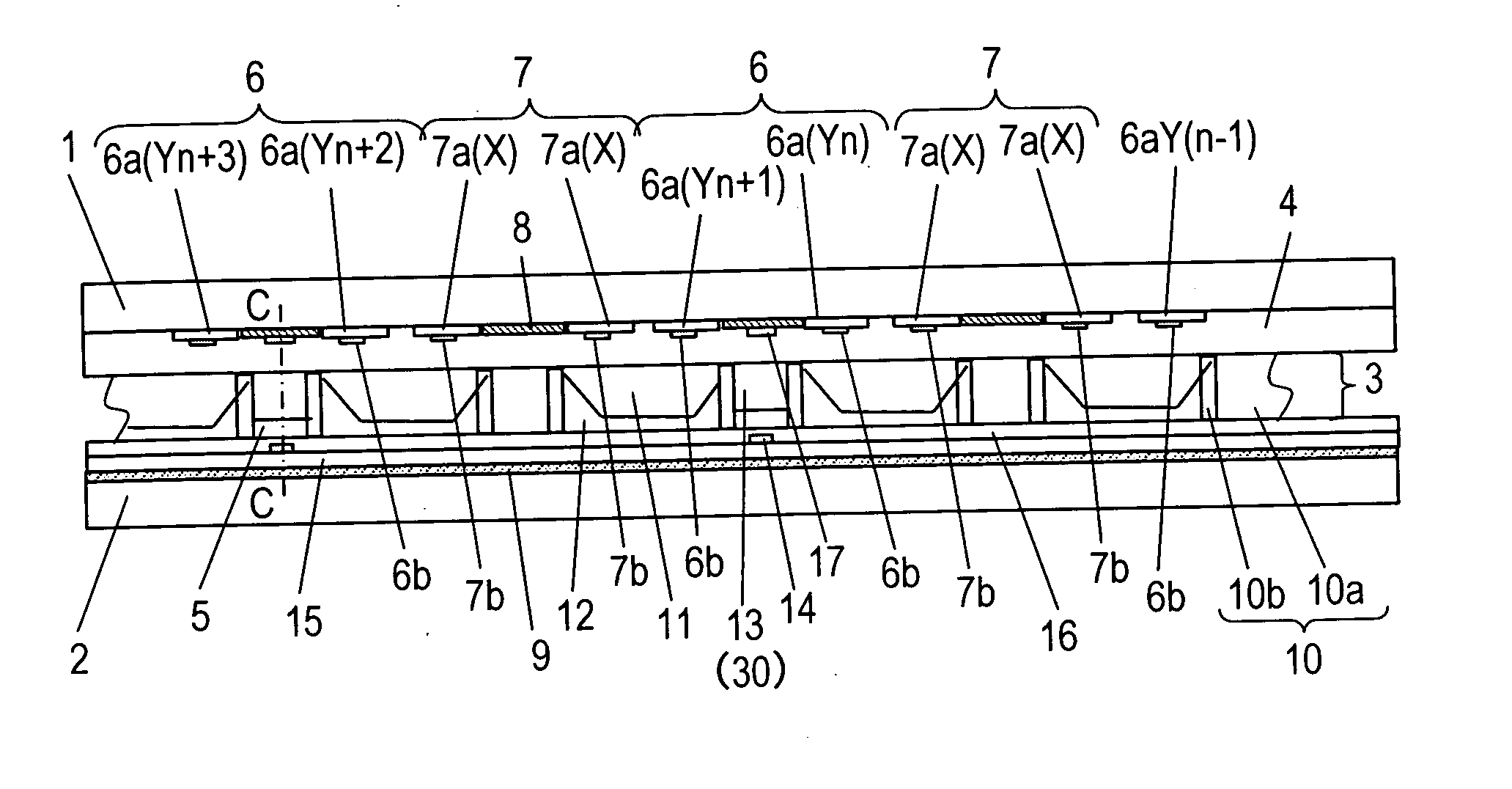
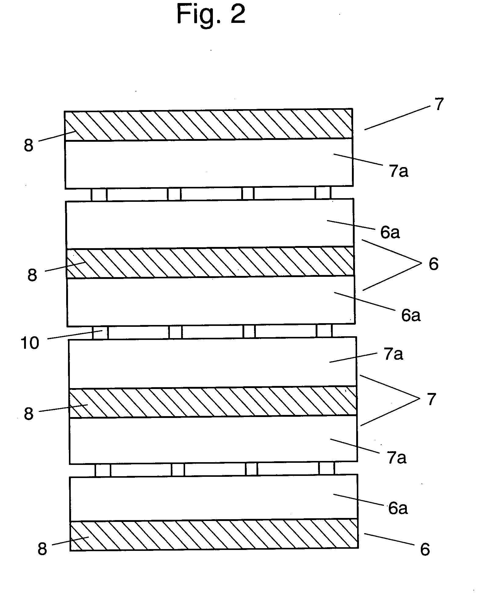
[0020]FIG. 1 is a cross sectional view of a PDP according to a first embodiment of the present invention, FIG. 2 is a schematic plan view showing an electrode arrangement on a front substrate side, which is a first substrate side, FIG. 3 is a schematic perspective view showing a back substrate side, which is a second substrate side and FIG. 4 is a plan view thereof.

[0021] As shown in FIG. 1, front substrate 1 which is a first substrate made of glass, and back substrate 2 which is a second substrate made of glass are disposed to face each other with discharge space 3 therebetween, and discharge space 3 is sealed with neon (Ne), xenon (Xe) and the like as gasses for irradiating ultraviolet rays by discharge. On front substrate 1, a group of belt-shaped electrodes consisting of pairs of scan electrodes 6 as first electrodes and sustain electrodes 7 as second electrodes are disposed in parallel with each other in such a manner as to be covered with dielectr...

second exemplary embodiment

(Second Exemplary Embodiment)

[0031]FIG. 6 is a cross sectional view showing a PDP according to a second embodiment of the present invention, and FIG. 5 is a cross sectional view depicting a discharge operation according to the second embodiment of the present invention.

[0032] The following is a description about the difference between the present embodiment and the first embodiment shown in FIG. 1. In the first embodiment, priming electrodes 14 are provided in priming discharge spaces 30 on back substrate 2, and during the address period, a priming discharge is formed between priming electrodes 14 and auxiliary electrodes 17 extending from scan electrodes 6. In the second embodiment shown in FIG. 6, on the other hand, no priming electrodes are provided in priming discharge spaces 30 on back substrate 2, and a priming discharge is performed during the initialization period between auxiliary electrodes 32 extended from scan electrodes 6, and data electrodes 9. Thus, the difference fr...


PUM


Abstract

A plasma display panel has address properties stabilized. A priming discharge is performed between auxiliary electrodes (17), which are formed on a front substrate (1) and coupled with scan electrodes (6) and priming electrodes (14) formed on a back substrate (2). Furthermore, a material layer (5) containing at least one of alkali metal oxide, alkaline earth metal oxide and fluoride is provided on regions corresponding to priming discharge spaces (30) (gap parts 13) on the back substrate (2). As a result, the priming discharge has a wider margin, and a supply of priming particles to the discharge cells is stabilized, whereby a discharge delay during the addressing is reduced, and the address properties are stabilized.

Description

TECHNICAL FIELD[0001] The present invention relates to plasma display panels used for wall-hung TVs and large-size monitors. BACKGROUND ART [0002] An AC surface discharge type plasma display panel (hereinafter referred to as PDP), which is a typical AC type PDP, is formed of a front plate made of a glass substrate having scan electrodes and sustain electrodes provided thereon for a surface discharge, and a back plate made of a glass substrate having data electrodes provided thereon. The front plate and the back plate are disposed to face each other in parallel in such a manner that the electrodes on both plates form a matrix, and that a discharge space is formed between the plates. And the outer part of the plates thus combined is sealed with a sealing member such as a glass frit. Between the substrates, discharge cells partitioned by barrier ribs are formed, and phosphor layers are provided in the cell spaces formed by the barrier ribs. In a PDP with this structure, ultraviolet ray...

Claims


Application Information

Patent Timeline
IPC IPC(8): H01J11/28H01J11/22H01J17/49
CPCH01J11/12H01J11/40H01J11/28H01J11/22
Inventor TACHIBANA, HIROYUKIMURAKOSO, TOMOHIRONOGUCHI, YASUYUKISHIRAI, TETSUYA
Owner PANASONIC CORP
Why Eureka
Try Eureka