Laser diode device

a laser diode and diode technology, applied in the direction of lasers, semiconductor laser structural details, semiconductor lasers, etc., can solve the problems of inpractical use and the size of the laser diode device b>10/b> is greater than 9 mm, and achieve the effect of convenient application

Active Publication Date: 2005-05-19
ARIMA LASERS CORP
View PDF4 Cites 25 Cited by
  • Summary
  • Abstract
  • Description
  • Claims
  • Application Information

AI Technical Summary

Benefits of technology

[0006] The present invention has been accomplished under the circumstances in view. It is one object of the present invention to provide a layer diode device, which uses a built-in automatic power control circuit instead of

Problems solved by technology

According to this design, the size of the laser diode device 10 is gr

Method used


Image

  • Laser diode device
  • Laser diode device
  • Laser diode device

Examples


Embodiment Construction

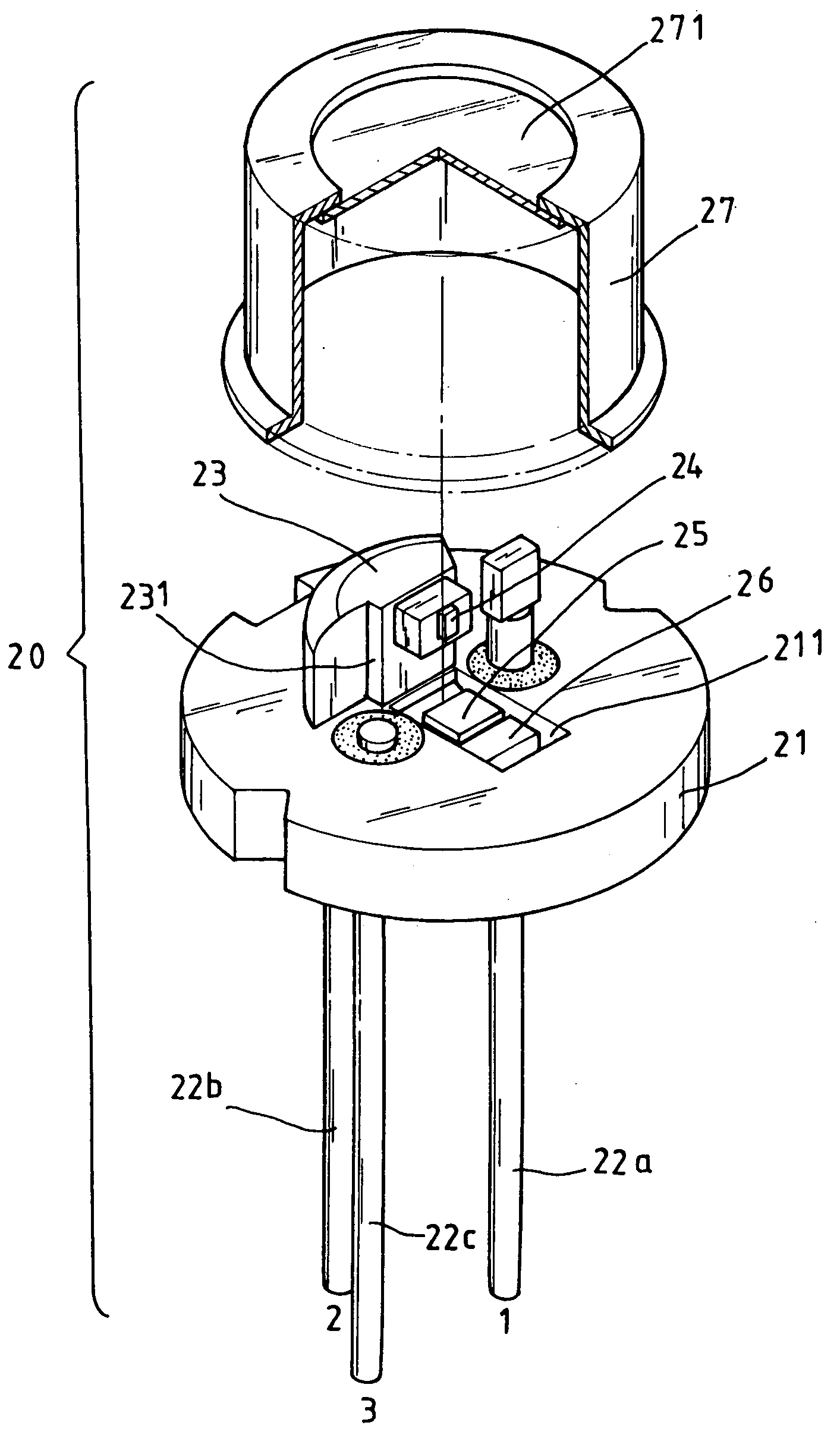
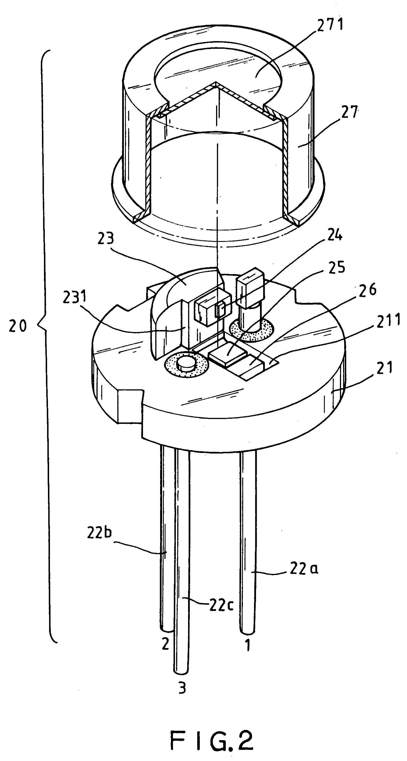
[0016] Referring to FIGS. 2˜4, a laser diode device 20 is shown comprising a heat sink 21, which has three pins, namely, the first pin 22a, the second pin 22b and the third pin 22c respectively extended from the back side, a mount (or stem) 23 provided at the front side of the heat sink 21 and connected to the second pin 22b for grounding, a submount 231 formed of a single chip silicon material and disposed at an inner side of the mount 23, a LD (laser diode) chip 24 bonded to the submount 231, a photo diode chip 25 mounted on the front side of the heat sink 21, a metal cap 27, which has a top glass window 271 and a bottom edge bonded to the heat sink 21, and an APC (automatic power control) circuit 26 made in the form of a circuit board or IC and encapsulated in the metal cap 27 and electrically connected to the pins 22a,22b,22c and the LD chip 24 and the PD chip 25 by wires 28 to form a laser diode voltage driving member.

[0017] Referring to FIGS. 4 and 5, the APC circuit 26 is en...


PUM


Abstract

A laser diode device of package not greater than 5.6 mm, having an automatic power control circuit directly mounted in a heat sink (or a submount) inside the metal cap thereof to substitute for an external circuit board for driving by voltage instead of current.

Description

BACKGROUND OF THE INVENTION [0001] 1. Field of the Invention [0002] The present invention relates to a laser diode device and, more particularly to such a laser diode device, which has an automatic power control circuit directly encapsulated in the heat sink (or submount) inside the metal cap for driving by voltage instead of current. [0003] 2. Description of the Related Art [0004] A laser semiconductor is a kind of diode, also called as a laser diode. Unlike regular diodes, a laser diode has the function of a laser oscillator. Therefore, a laser diode has the electric properties of regular diodes and the optical property of emitting a laser light as a laser oscillator does. A laser oscillator is an object (media) that causes a laser effect. It can be seen in gas form, liquid form, or semiconductor form. Ruby laser device is a solid laser device. Helium-neon laser device is a gas form laser device that emits red laser light. Chromatic laser device is a typical liquid form laser devi...

Claims


Application Information

Patent Timeline
IPC IPC(8): H01S5/022H01S3/04H01S5/02H01S5/024H01S5/06H01S5/0683
CPCH01S5/02212H01S5/02248H01S5/042H01S5/0683H01L2224/48137H01L2224/49113H01L2224/48091H01L2924/00014H01S5/02325
Inventor SIMOUN-OU, SZUTSUNYEN, HSIEN-CHENG
Owner ARIMA LASERS CORP
Why Eureka
Try Eureka