Method of manufacturing semiconductor device and method of treating semiconductor surface

Inactive Publication Date: 2005-05-19
FUJI ELECTRIC CO LTD
View PDF2 Cites 17 Cited by
  • Summary
  • Abstract
  • Description
  • Claims
  • Application Information

AI Technical Summary

Benefits of technology

[0026] According to the invention, silicon atoms migrate during the step of annealing, so that the gate insulator film forming region such as the trench sidewall or the wafer surface is planarized in the atomic level, thereby obtaining the flat semiconductor surface with the standard deviation of roughness Rms less than 0.5. When the trench is formed in the semico

Problems solved by technology

Due to the variation, it is difficult to accurately position the mask used in the following step, thereby making it difficult to obtain a fine structure.
However, in the method described in the above identified patent application, it is sti

Method used


Image

  • Method of manufacturing semiconductor device and method of treating semiconductor surface
  • Method of manufacturing semiconductor device and method of treating semiconductor surface
  • Method of manufacturing semiconductor device and method of treating semiconductor surface

Examples


Embodiment Construction

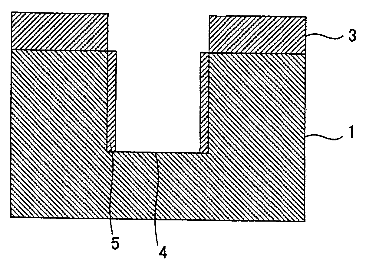
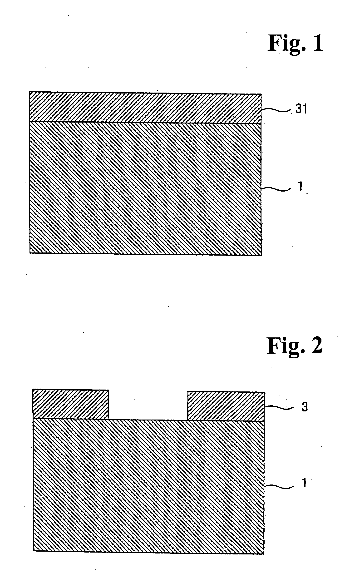
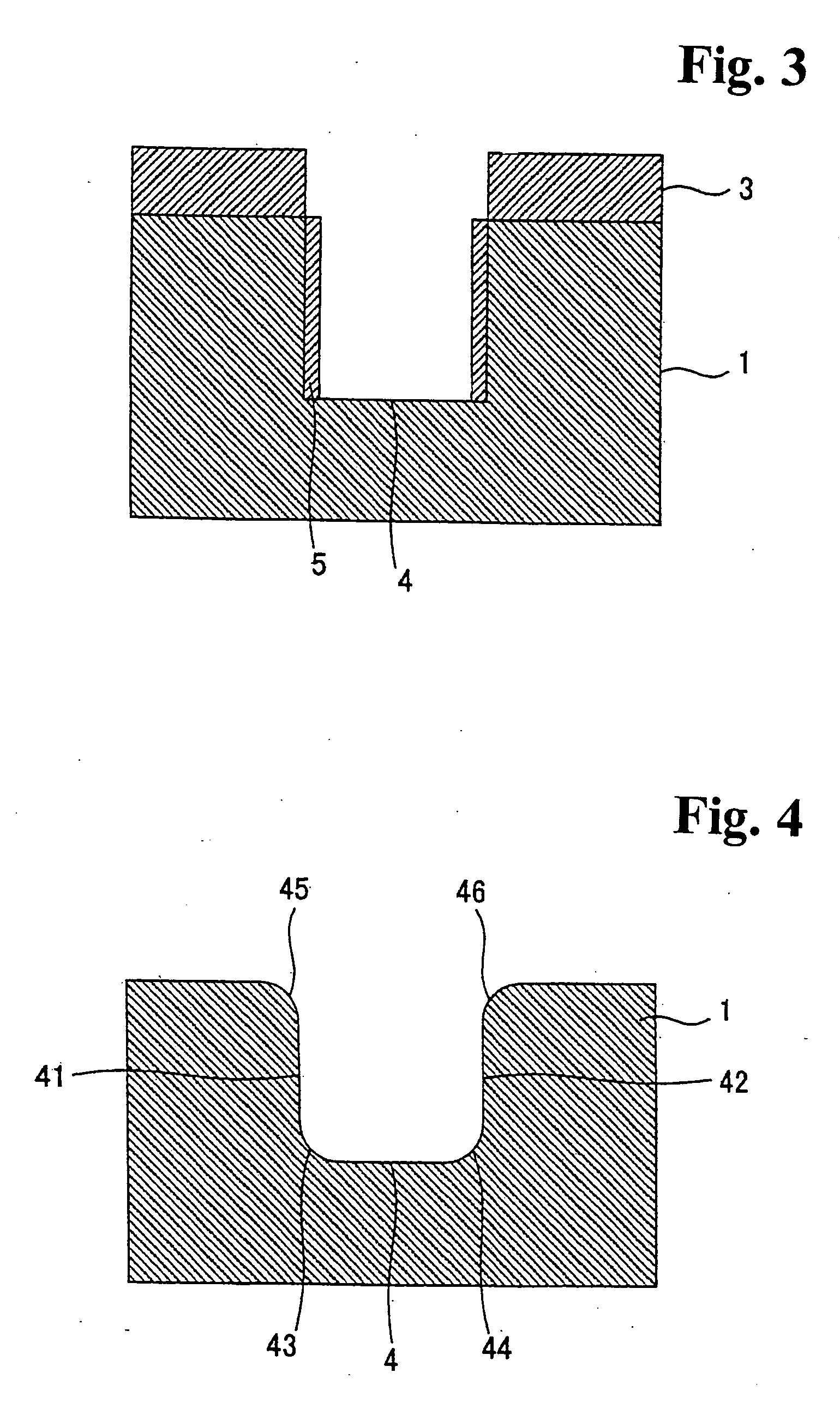
[0053] Hereunder, embodiments of the invention will be described in detail with reference to the accompanied drawings. FIGS. 1 through 5 are schematic cross sectional views showing arrangements of a trench MOS semiconductor device in manufacturing steps according to an embodiment of the invention. First, a well region (not shown) is formed in a silicon semiconductor substrate 1 through a conventional manufacturing method of a trench MOS semiconductor device. Then, a silicon oxide film 31 is formed on the semiconductor substrate 1 as a mask.

[0054] A mask (not shown) formed of a photo resist having a pattern with an opening is formed on the silicon oxide film 31 for forming a trench forming region. The silicon oxide film 31 is etched using the resist mask to form a mask 3 having a predetermined trench pattern as shown in FIG. 2. A trench 4 is formed in the semiconductor substrate 1 by etching the semiconductor substrate with reactive ion etching (RIE) technique using the mask 3. Upon...


PUM


Abstract

A method of manufacturing a semiconductor device includes the steps of: exposing a semiconductor surface of a substrate; annealing the substrate in a hydrogen atmosphere at a hydrogen pressure between 200 Torr and 760 Torr and a temperature between 1000° C. and 1050° C. to planarize the exposed semiconductor surface; and forming a gate insulator film on the planarized semiconductor surface.

Description

BACKGROUND OF THE INVENTION AND RELATED ART STATEMENT [0001] The present invention relates to a method of manufacturing a semiconductor device and a method of treating semiconductor surface including a step of annealing a semiconductor to planarize an exposed surface of the semiconductor. Specifically, the present invention relates to a method including a step of planarizing a region where a gate insulator film is formed before forming the gate insulator film; and a method including a step of planarizing a sidewall of a trench formed in a semiconductor substrate and rounding a corner of the trench simultaneously. [0002] Conventionally, a semiconductor device manufactured by utilizing a trench includes a semiconductor device with a structure having a gate insulator film formed in a trench (hereinafter referred to as a trench MOS semiconductor device). Usually, the trench MOS semiconductor device is manufactured through a step of forming a gate insulator film in a trench after a step ...

Claims


Application Information

Patent Timeline
IPC IPC(8): H01L21/28H01L21/316H01L21/3205H01L21/324H01L21/336H01L21/44H01L21/4763H01L29/423H01L29/78
CPCH01L21/28167H01L29/4236H01L21/324H01L21/3247
Inventor HIRUTA, REIKOKURIBAYASHI, HITOSHISHIMIZU, RYOSUKE
Owner FUJI ELECTRIC CO LTD
Why Eureka
Try Eureka