

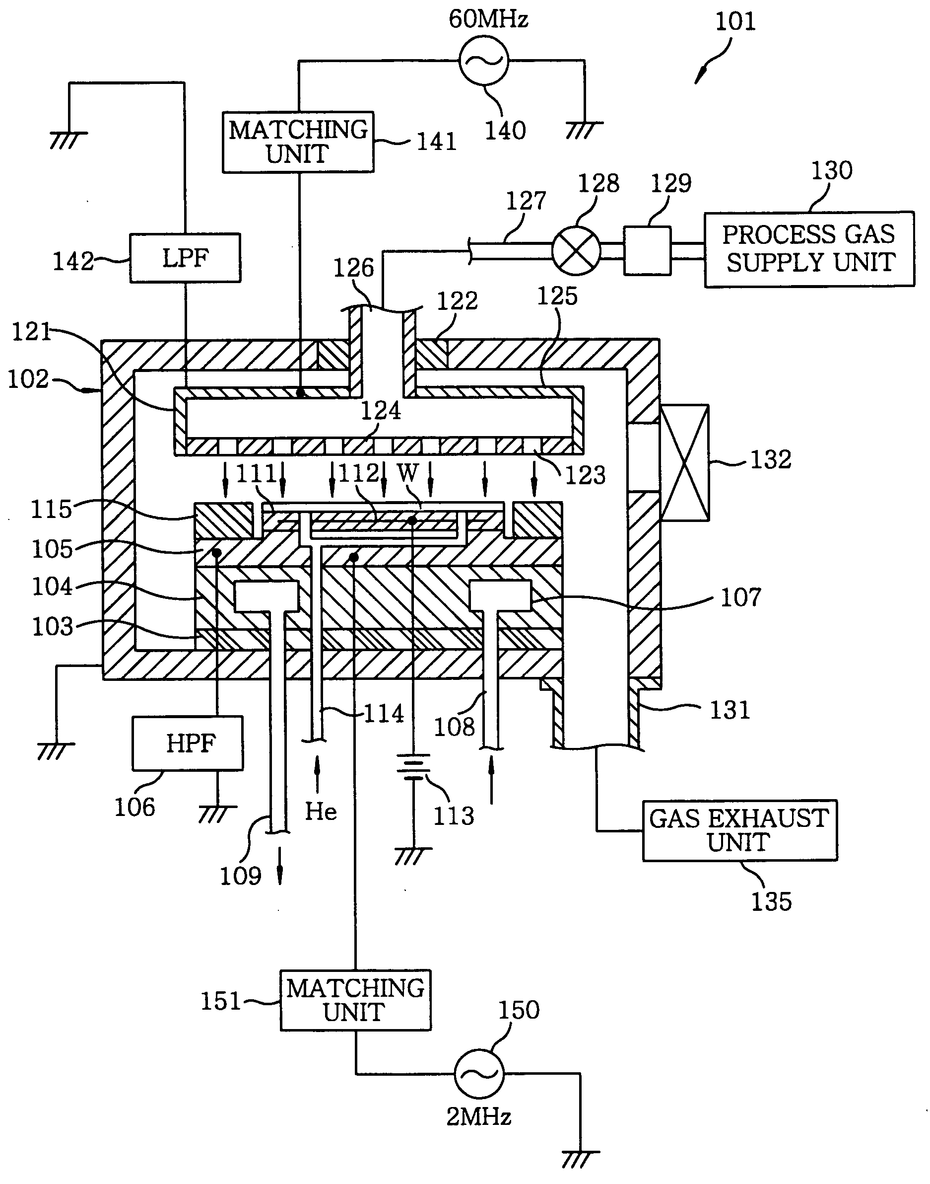
Plasma ashing method
a technology of plasma and ashing film, applied in the direction of photosensitive material processing, electrical equipment, electric discharge tubes, etc., can solve the problems of increasing the dielectric constant (k value) of the low-k film, hybrid ashing can inflict damage on the low-k film, and the performance of a semiconductor is lower, so as to achieve the effect of efficient removal of the resist film
- Summary
- Abstract
- Description
- Claims
- Application Information
AI Technical Summary
Benefits of technology
Problems solved by technology
Method used
Image

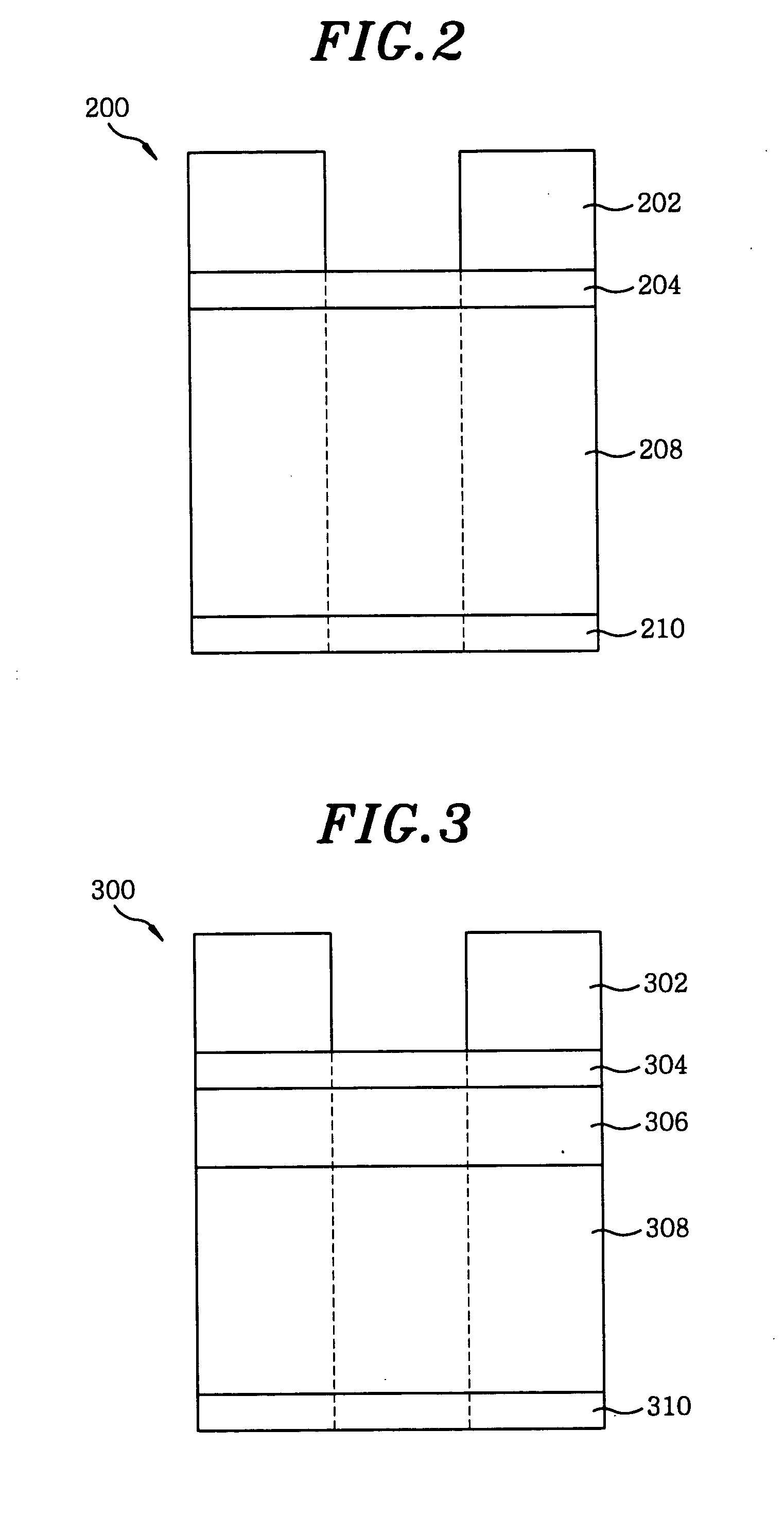
Examples
experiment 4
[0190] B8. Dependence on a First High Frequency Electric Power
[0191] In this experiment, the same plasma ashing process performed in the experiment 1 was carried out with the pressure in the chamber 404 fixed at 50 mTorr while varying a first high frequency (100 MHz) electric power, other conditions remaining the same as in the experiment 1. A result of the experiment 4 is described in Table 4. Further, a second high frequency (3.2 MHz) electric power was set to be 0 W (i.e., the second electric power supply 428 does not output the second high frequency electric power).
TABLE 4First high frequencyelectric power (W)30010002500Second high frequency electric000power (W)In-chamber pressure (mTorr)555Ashing time (sec)1885832Processing gas (O2) flow rate200200200(sccm)Δd1t191315Δd1m16159Δd1b19159ΔE223033
[0192] As the first high frequency electric power applied to the lower electrode 406 increases, the CD shift (an average value of Δd1t, Δd1m and Δd1b) of the low-k film 208 decreases, an...
PUM
 Abstract
Description
Claims
Application Information