Apparatus and method for processing a microelectronic workpiece using metrology

a microelectronic and workpiece technology, applied in the direction of machining electric circuits, semiconductor/solid-state device testing/measurement, instruments, etc., can solve the problems of corresponding decrease in manufacturing tolerances that must be met by manufacturing tools, and achieve rapid and low-cost experimentation, wide range of process sequence and control flexibility, and easy interchange of chemistries

Inactive Publication Date: 2005-05-19
SEMITOOL INC
View PDF62 Cites 8 Cited by
  • Summary
  • Abstract
  • Description
  • Claims
  • Application Information

AI Technical Summary

Benefits of technology

[0026] An alternate exemplary embodiment of the tool incorporating the present invention is a process development configuration. This tool design is directed to developing optimized processes. The configuration allows a wide range of flexibility in process sequence and control. For example, a process engineer might want to measure incoming seed layer thickness, ECD seed layer deposition results, ECD fill results, and post annealing results. Since the plating solution reservoirs can be much smaller, the user may also quickly and easily interchange chemistries for rapid and low-cost experimentation. The user may want to run split lots with a wide variety of process combinations to determine feasibility of a production process.

Problems solved by technology

As the size of various microelectronic circuits and components decreases, there is a corresponding decrease in the manufacturing tolerances that must be met by the manufacturing tools.

Method used


Image

  • Apparatus and method for processing a microelectronic workpiece using metrology
  • Apparatus and method for processing a microelectronic workpiece using metrology
  • Apparatus and method for processing a microelectronic workpiece using metrology

Examples


Embodiment Construction

[0040] While this invention is susceptible of embodiment in many different forms, there are shown in the drawings and will be described herein in detail, specific embodiments thereof with the understanding that the present disclosure is to be considered as an exemplification of the principles of the invention and is not intended to limit the invention to the specific embodiments illustrated.
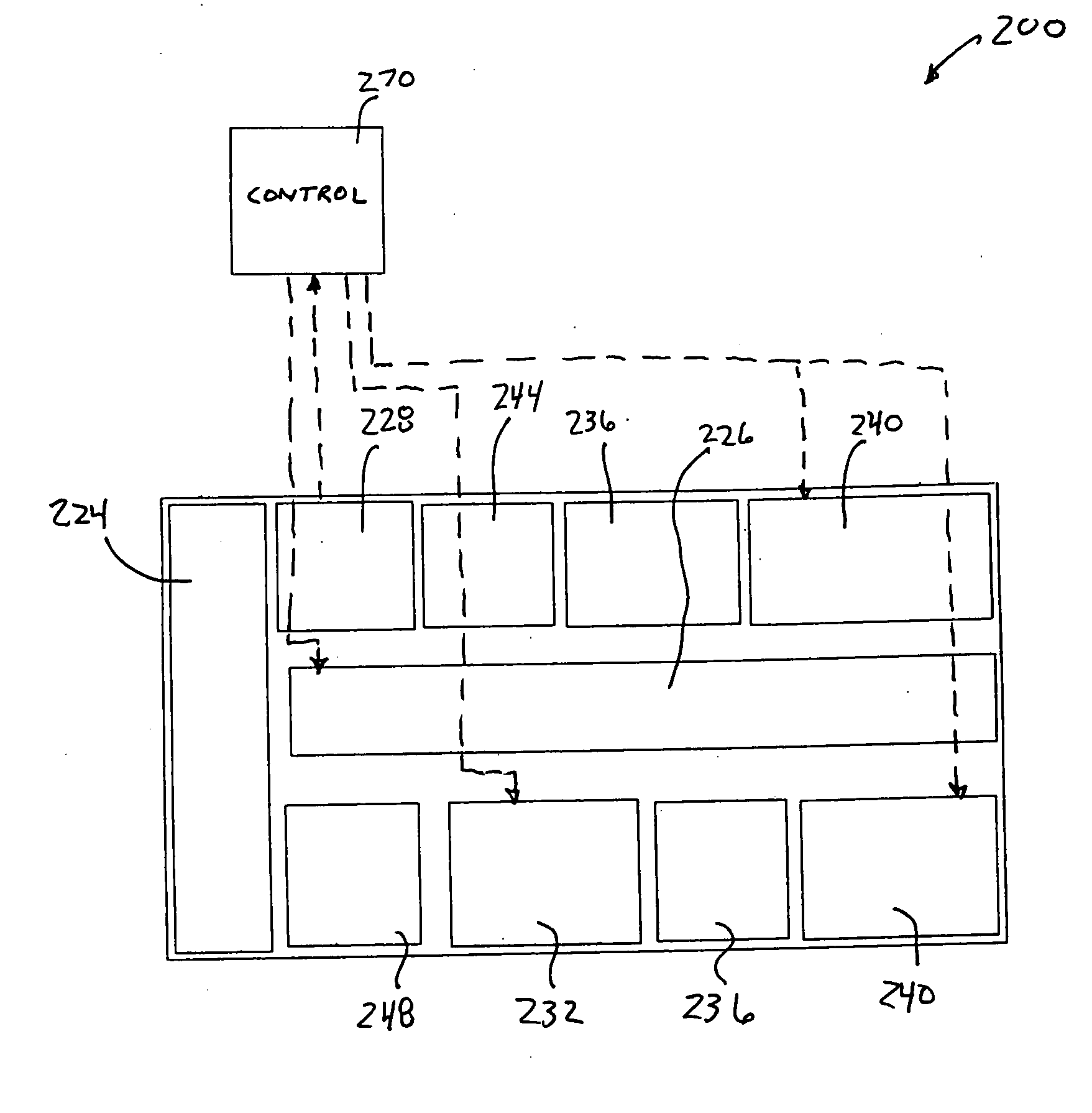
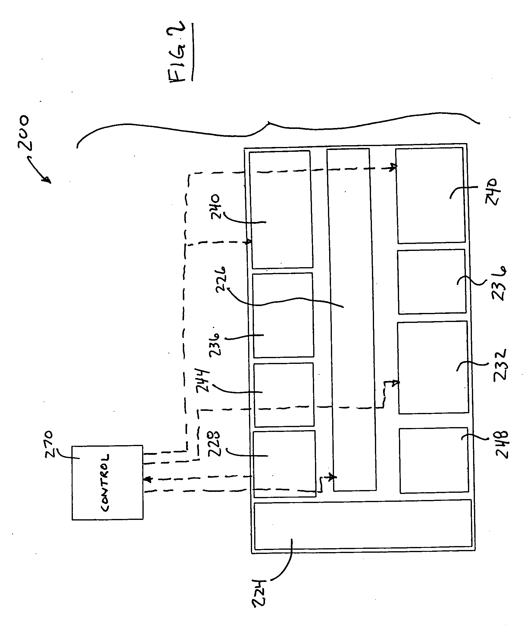
[0041] Systems

[0042] Integrated Processing Tool

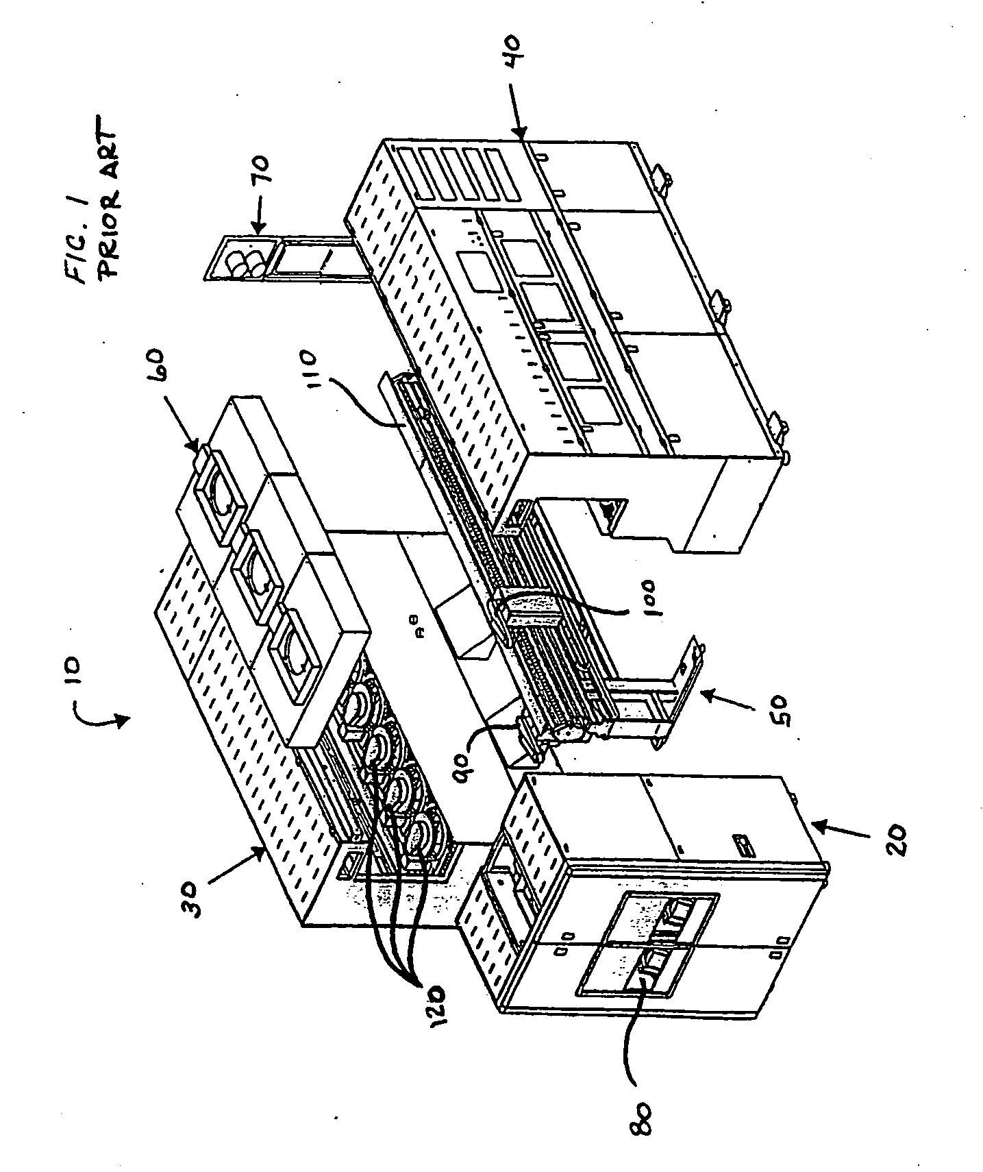
[0043]FIG. 1 is an exploded isometric view of a prior art integrated microelectronic workpiece-processing tool 10. This exemplary tool embodiment is disclosed in U.S. patent application Ser. No. 08 / 991,062, filed Dec. 15, 1997, entitled “Semiconductor Processing Apparatus Having Lift and Tilt Mechanism.”

[0044] Although modularity is not necessary to the overall tool function, the tool 10 is shown as having been separated into individual modular components. The exemplary integrated microelectronic workpiece processing tool 10 of FIG. 1 comprises an...


PUM

PropertyMeasurementUnit
currentaaaaaaaaaa
thicknessaaaaaaaaaa
conductiveaaaaaaaaaa

Abstract

A processing apparatus for processing a microelectronic workpiece includes a metrology unit and a control, signal-connected to the metrology unit. The control can modify a process recipe or a process sequence of the processing apparatus based on a feed forward or a feed back signal from the metrology unit. A seed layer deposition tool, a process layer electrochemical deposition tool, and a chemical mechanical polishing tool, arranged for sequential processing of a workpiece, can be controlled as an integrated system using one or more metrology units. A metrology unit can be located at each tool to measure workpiece parameters. Each of the metrology units can be used as a feed forward control and/or a feed back control at each of the tools.

Description

BACKGROUND OF THE INVENTION [0001] The present invention is directed to an apparatus and method for processing a microelectronic workpiece. More particularly, the present invention is directed to an improved apparatus and method of processing a microelectronic workpiece using a metrology result representative of a microelectronic workpiece condition. For purposes of the present application, a microelectronic workpiece is defined to include a microelectronic workpiece formed from a substrate upon which microelectronic circuits or components, data storage elements or layers, and / or micro-mechanical elements are formed. [0002] The fabrication of microelectronic components from a microelectronic workpiece, such as a semiconductor wafer substrate, polymer or ceramic substrate, etc., involves a substantial number of operations performed on the microelectronic workpiece. Such operations include, for example, material deposition, patterning, doping, chemical mechanical polishing, electropol...

Claims


Application Information

Patent Timeline
Patent Type & Authority Applications(United States)
IPC IPC(8): H01L21/00
CPCH01L21/67103H01L21/67173H01L21/67276H01L21/67219H01L21/67253H01L21/67207
Inventor RITZDORF, THOMAS L.EUDY, STEVE L.WILSON, GREGORY J.MCHUGH, PAUL R.
Owner SEMITOOL INC
Why Eureka
Try Eureka