Circuit board with localized stiffener for enhanced circuit component reliability

a circuit board and localized technology, applied in the direction of printed circuit stress/warp reduction, printed circuit non-printed electric components association, semiconductor/solid-state device details, etc., can solve the problems of less compliant solder joints, reduced device standoff height, and crowded joints along the edges of chips, so as to increase the thermal cycle fatigue life of one or more solder joints

Inactive Publication Date: 2005-05-26
RPX CORP
View PDF7 Cites 20 Cited by
  • Summary
  • Abstract
  • Description
  • Claims
  • Application Information

AI Technical Summary

Benefits of technology

[0007] The present invention is directed to a circuit board assembly comprising a laminate substrate and a surface mount device having a CTE less than that of the laminate substrate and attached with at least one solder joint to a first surface of the laminate substrate. According to the invention, the circuit board assembly includes a localized stiffener attached to a second surface of the laminate substrate so as to be directly opposite the circuit device. The localized stiffener is formed of a material and is shaped so that, when appropriately attached to the laminate substrate, is capable of increasing the thermal cycle fatigue life of the one or more solder joints that attach the device to a laminate substrate. For this purpose, the localized stiffener has at least one lateral dimension in a plane parallel to the first and second surfaces of the laminate substrate that is greater than a corresponding lateral dimension of the device. Furthermore, the CTE of the localized stiffener is less than the CTE of the laminate substrate, and the modulus of elasticity of the localized stiffener is equal to or greater than that of the laminate substrate.
[0008] According to the invention, the localized stiffener is able to increase the longevity of a surface-mount device mounted to a laminate substrate by locally inhibiting the thermal expansion and shrinkage of a region of the substrate directly beneath the device, thereby reducing the stresses on the one or more solder joints that attach the device to the substrate. Such improvements can be achieved in combination with more conventional approaches, such as device underfilling, modified solder compositions, and thinner laminate substrates. The localized stiffener can also be utilized to reduce yield losses attributable to excessive warpage and stresses that can occur during the circuit board assembly process.

Problems solved by technology

Due to the numerous functions typically performed by the microcircuitry of a flip chip, a relatively large number of solder joints are typically required, resulting in the joints being crowded along the edges of the chip.
To reduce device profile and the overall size of circuit board assemblies, a current IC packaging trend is for smaller solder joints to reduce bump pitch, which also reduces device standoff height resulting in solder joints that are less compliant.
Such size constraints result in solder joints of minimal size and therefore reduced strength.
A CTE mismatch particularly exists for flip-chip-on-board (FCOB) processes in which a flip chip is mounted to an organic laminate circuit board, such as a printed wiring board (PWB) or printed circuit board (PCB).
Thermal stresses arising from this CTE mismatch can potentially fatigue and fracture the solder joints, particularly if the device is subject to many temperature excursions, high temperatures, and / or intense vibration.

Method used


Image

  • Circuit board with localized stiffener for enhanced circuit component reliability
  • Circuit board with localized stiffener for enhanced circuit component reliability

Examples


Embodiment Construction

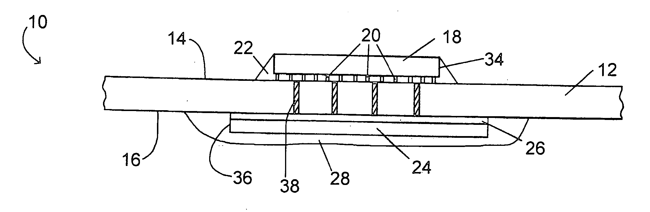
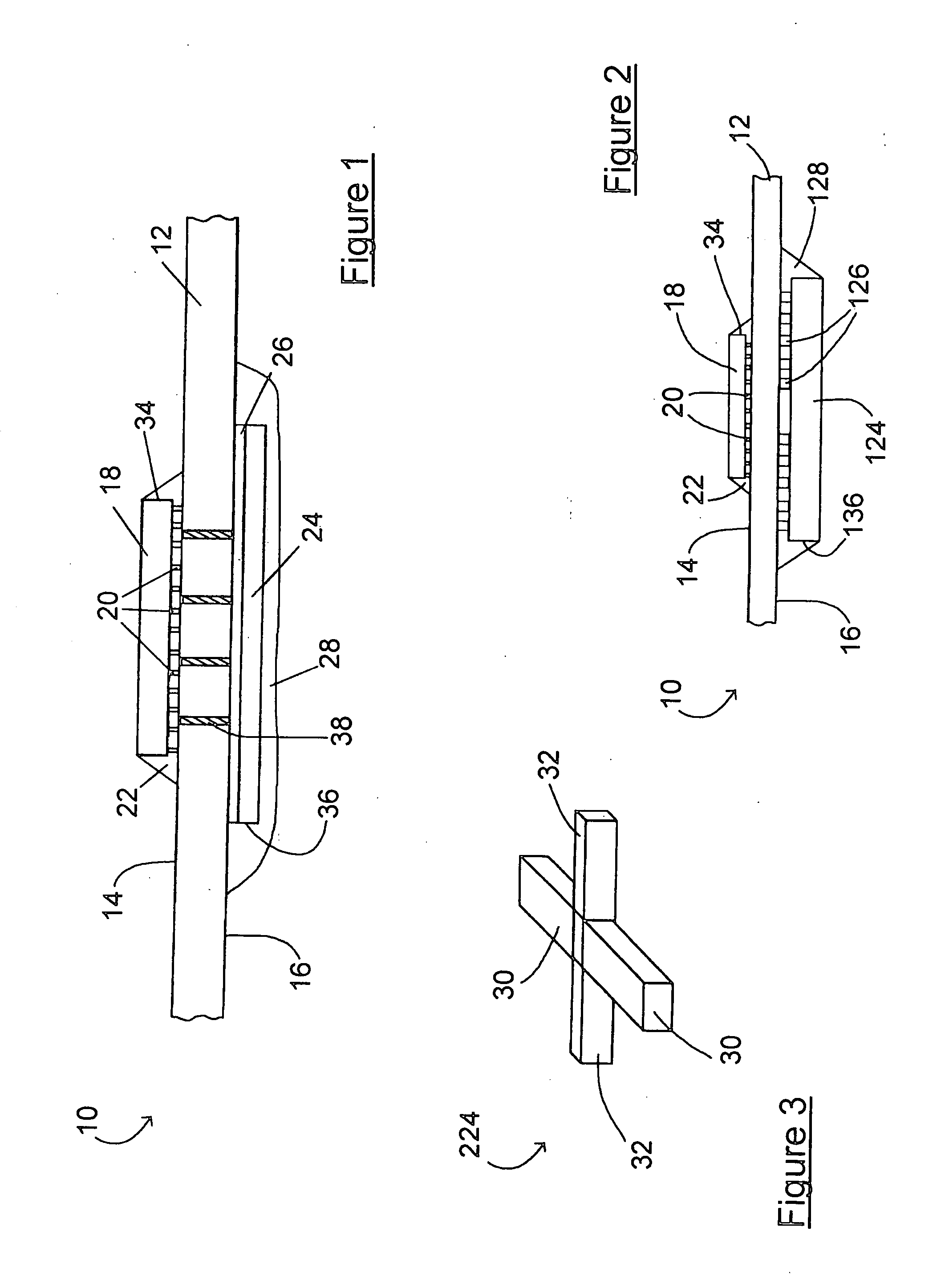
[0013]FIG. 1 represents a portion of a circuit board assembly 10 comprising a substrate 12 on whose surface 14 a surface mount component 18, such as a flip chip, is attached. The substrate 12 is a laminate organic substrate, such as a printed circuit board (PCB) or a printed wiring board (PWB). An example of a suitable substrate material is known as FR-4, available in various thicknesses (e.g., about 0.015 to about 0.065 inch (about 0.38 to about 1.65 mm)) and typically having a CTE of about 17 ppm / EC in the plane of the substrate. FR-4 boards are typically a glass-reinforced or woven fiberglass-reinforced epoxy resin laminate available from various sources.

[0014] As known in the art, the component 18 may be formed of a semiconductor material, such as silicon, in whose surface integrated circuits are formed. Other potential materials for the component 18 include alumina, beryllia, quartz, etc. As is conventional, the component 18 is electrically and physically connected by a number...


PUM


Abstract

A circuit board assembly comprising a laminate substrate and a surface mount device having a CTE less than that of the laminate substrate and attached with at least one solder joint to a first surface of the laminate substrate. The assembly further includes a localized stiffener attached to a second surface of the laminate substrate so as to be directly opposite the circuit device. The localized stiffener is formed of a material and is shaped so that, when attached to the laminate substrate, the stiffener is capable of increasing the thermal cycle fatigue life of the one or more solder joints that attach the device to the substrate.

Description

BACKGROUND OF THE INVENTION [0001] (1) Field of the Invention [0002] The present invention generally relates to surface-mount circuit devices. More particularly, this invention relates to a laminate circuit board substrate modified to have a localized stiffener on a surface opposite a surface-mount circuit device so as to improve the fatigue life of one or more solder joints securing the device to the substrate. [0003] (2) Description of the Related Art [0004] Electronic circuit assemblies are often required to be capable of surviving in hostile operating environments, including those commonly found in automotive and aerospace applications. Such assemblies often employ surface-mount (SM) integrated circuit (IC) devices, which are generally characterized as being electrically and mechanically attached to the substrate of a circuit assembly with one or more terminals or leads that are soldered to conductors on the substrate surface. A prominent example of a SM IC device is a flip chip...

Claims


Application Information

Patent Timeline
Patent Type & Authority Applications(United States)
IPC IPC(8): H05K1/02H05K3/00
CPCH05K1/0206H05K1/0271H05K3/0061H05K2201/2009H05K2201/10204H05K2201/10545H05K2201/10674H05K2201/068H01L2224/73204H01L2224/16225
Inventor CHENGALVA, SURESH K.IHMS, DAVID W.MYERS, BRUCE A.
Owner RPX CORP
Why Eureka
Try Eureka