

Methods of direct growth of carbon nanotubes on catalytic surfaces
a technology of carbon nanotubes and catalytic surfaces, which is applied in the direction of material nanotechnology, coatings, textiles and papermaking, etc., can solve the problems of limited field and thermionic emission of nanotube devices, limited application prospects, and limited synthesis of robust materials
Inactive Publication Date: 2005-05-26
VANDERBILT UNIV
View PDF4 Cites 30 Cited by
- Summary
- Abstract
- Description
- Claims
- Application Information
AI Technical Summary
Benefits of technology
[0011] It is another object of the present invention to provide for the preparation of a conductin
Problems solved by technology
This need derives from the well documented limitations of patterning and robust material synthesis technologies as device dimensions decrease below 100 nm.
While little doubt now exists that CNT transistors will eventually provide superior functional performance to CMOS for many applications, considerable uncertainty remains regarding the ability to create practical alternative devices from CNT transistor circuits.
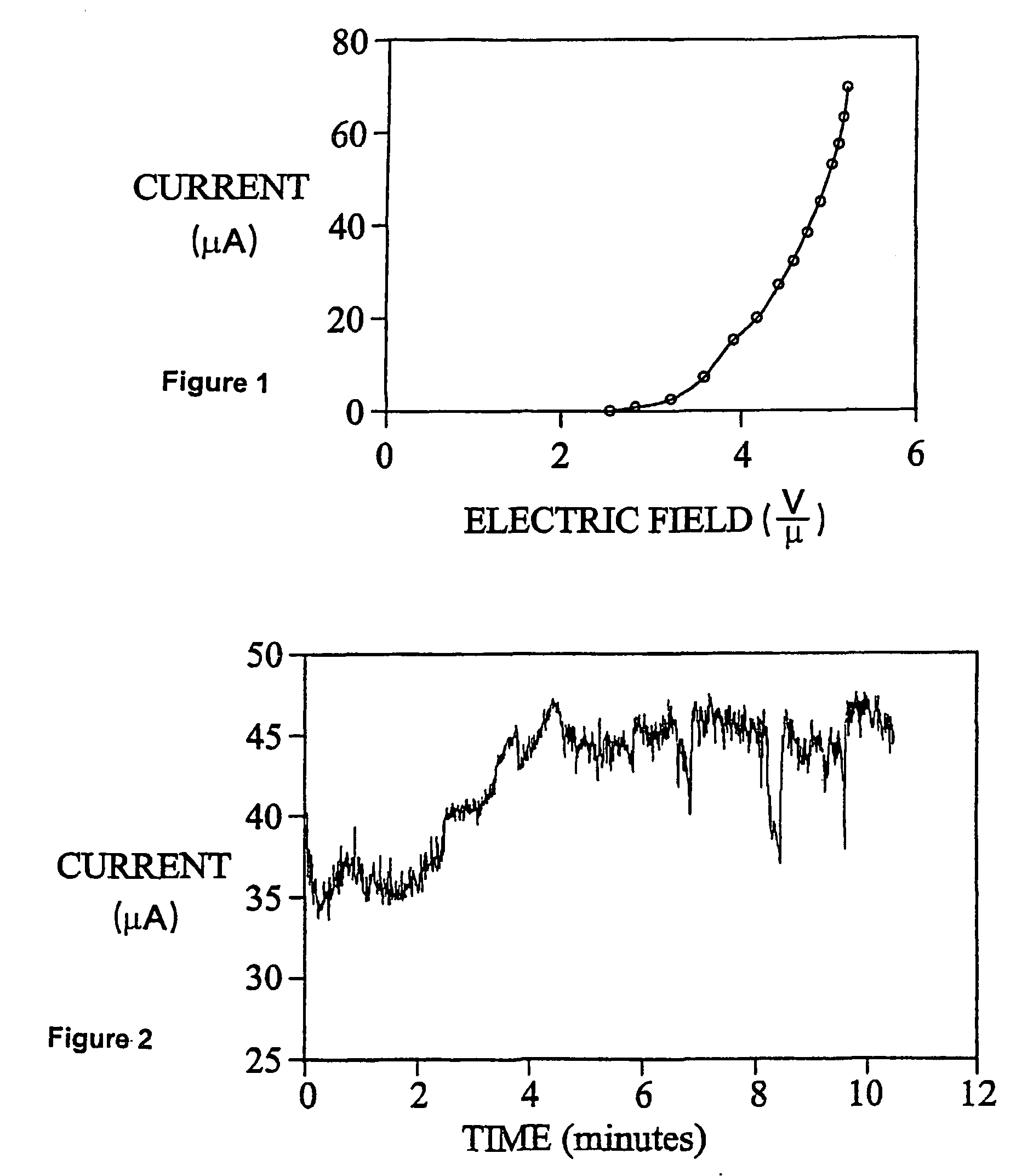
The turn on voltage was reasonable at 3 Vμ−1, however, the plot in FIG. 2 of emission current with time shows the present limitation of nanotube devices for field and thermionic emission.
Currently, these structures lack the ability to emit stably over time.
This behavior is believed to be due to less than optimal coupling of the CNT to the substrate.
The major disadvantage to these approaches is that the base support for the nanotube bundles is an insulator.
While it may be possible to etch away insulating substrates and attach nanotube arrays to conducting substrates, such a methoding step increases the cost and complexity of the fabrication of nanotube devices.
The diffusion of the reactive carbon source is thought to be a rate-limiting step.
Method used
View moreImage
Smart ImageViewing Examples

Examples
example
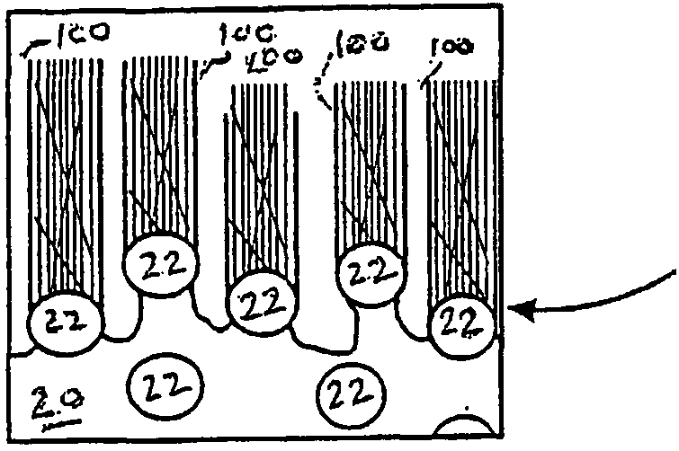
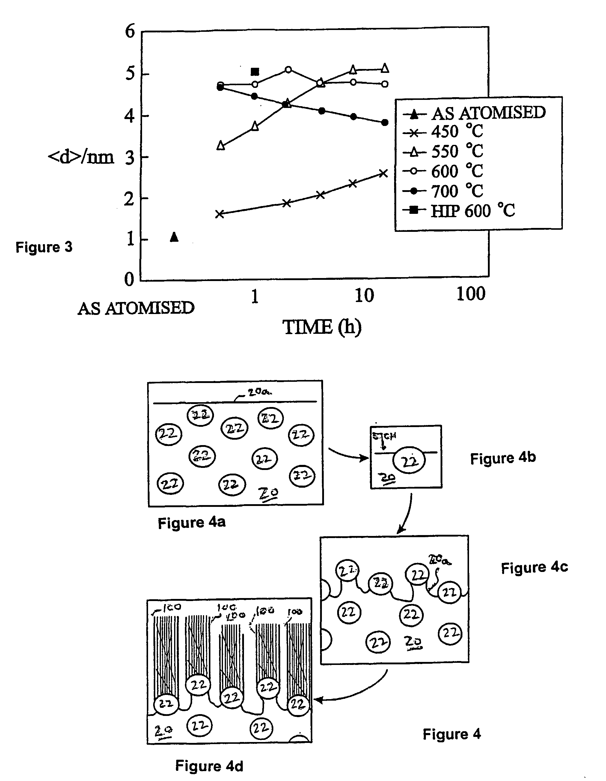
[0048] A sample is prepared by successively sputtering 1000 angstroms of Cu, 150 angstroms of Co and another 1000 angstroms of Cu on a silicon substrate with native oxide coating. The wafer is heat treated at 450° C. for 40 minutes to form Co precipitates. The wafer is then etched in 5 vol. % HNO3 in water to reveal the Co precipitates. CNTs are then grown on the surface of the wafer by plasma enhanced CVD. A photomicrograph of the CNTs is shown in FIGS. 8 and 9. These tubes have been imaged by transmission electron microscopy and an example of one of the tubes is shown in the photomicrograph of FIG. 10. The fringes from the walls of the nanotube are clearly visible.
Login to View More PUM
 Abstract
The present invention uses a conductor as a catalytic support for carbon nanotube growth. The use of conductive catalytic support will provide a contact to the nanotubes with low resistance. Carbon nanotubes grown on insulators must be modified to allow good connections. Second, creation of catalytic particles has been largely accomplished by precipitation of transition metals from salt solutions or thermal decomposition of thin films, while the present method uses precipitation from a solid solution. This will allow better control of the size distribution of catalysts. The precipitates will be coherent with the support allowing good anchoring of the catalysts for base growth of carbon nanotubes. Third, the approach is amenable to patterning by photolithography or other means of applying copper / transition metal thin films.
Description
TECHNICAL FIELD [0001] The present invention provides a method for synthesis of carbon nanotubes on an electrically conductive support, such as copper. More particularly, the present invention relates to synthesis of carbon nanotube transistors directly on a patternable support, suitable for ultra large scale integration (ULSI) patterning and interconnection. BACKGROUND ART [0002] The 1999 International Technology Roadmap for Semiconductors (ITRS) identifies a pressing need “to investigate new devices that may provide a more cost-effective alternative to planar CMOS” in the next 10-15 years. This need derives from the well documented limitations of patterning and robust material synthesis technologies as device dimensions decrease below 100 nm. Carbon nanotube (CNT) transistors are a particularly promising alternative device technology. Recent work has demonstrated their efficacy as field-effect transistors, and the selective patterning of semiconducting CNTs. While little doubt now...
Claims
Login to View More Application Information
Patent Timeline
 IPC IPC(8): D01F9/127
CPCD01F9/127B82Y30/00
InventorHOFMEISTER, WILLIAM
OwnerVANDERBILT UNIV