Method for anodic bonding of wafers and device

a technology of anodic bonding and wafers, applied in the manufacture of microstructural devices, electrical apparatus, semiconductor devices, etc., can solve the problems of limited thickness of useful silicon layer and oxide layer, high cost of simox method, and inability to produce thick layers and planar surfaces. to achieve the effect of preventing bond defects

Inactive Publication Date: 2005-05-26
ROBERT BOSCH GMBH
View PDF19 Cites 32 Cited by
  • Summary
  • Abstract
  • Description
  • Claims
  • Application Information

AI Technical Summary

Benefits of technology

[0012] It is furthermore advantageous that the intermediate layer is formed such that it plastically encloses any particles present and evens out height differences of the bonded surfaces. This ensures that no extensive bond defects occur during bonding.
[0013] It is particularly advantageous that second wafer (1, 100, 200, 300) may have several layers, in particular a silicon substrate (1) and further layers (3, 4, 403). If these layers are structured in some way, the intermediate layer is able to even out any height differences of the surfaces caused by structuring and thus prevent bond defects.
[0014] In another particularly advantageous embodiment of the present invention, an electrically insulated conductive layer is produced on the silicon functional layer of the second wafer. This conductive layer may be structured to form printed conductors, which are locally bonded to the functional layer. They establish the electrical connection between the electromechanical structures of an MEMS component, which are not defined until the base wafer and the functional layer are joined. By combining several structured conductive and insulating layers, there is a possibility to establish almost any electrical connection within the bond surface, so that even more complex sensor structures, for example, having intersecting printed conductors, may be designed. In addition, buried printed conductors allow flat surfaces to be formed on the top of the functional layer, so that known encapsulating methods such as bonding may be used.

Problems solved by technology

Advantages compared to thin-film technologies, with the exception of polysilicon epitaxy, include the absence of a stress gradient, and the possibility of producing thick layers and planar surfaces.
The SIMOX method is very expensive because it needs equipment for high-current oxygen implantation.
In addition, in this method the thickness of the useful silicon layer and of the oxide layer is limited.
Another constructive limitation of the SIMOX method is that it is not possible to run buried printed conductors underneath the functional layer.
Encapsulation of the micromechanical components is thus made considerably more difficult because it is then impossible to provide a topography-free bond frame for the cap in a simple manner.
The problem in any direct bonding method is the yield and therefore the cost.
Direct bonding methods are highly sensitive to particles which result in extensive bond occlusions.
Therefore, significant yield losses are to be expected when the oxide layer is structured.
In the direct bonding method it is not possible to run buried printed conductors underneath the functional layer, because extensive bond defects may occur due to the topography.
This in turn makes encapsulation difficult.

Method used


Image

  • Method for anodic bonding of wafers and device
  • Method for anodic bonding of wafers and device
  • Method for anodic bonding of wafers and device

Examples


Embodiment Construction

[0041] The present invention is described in detail with reference to the following exemplary embodiments.

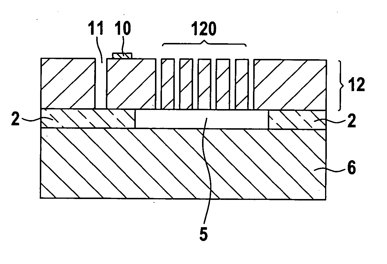
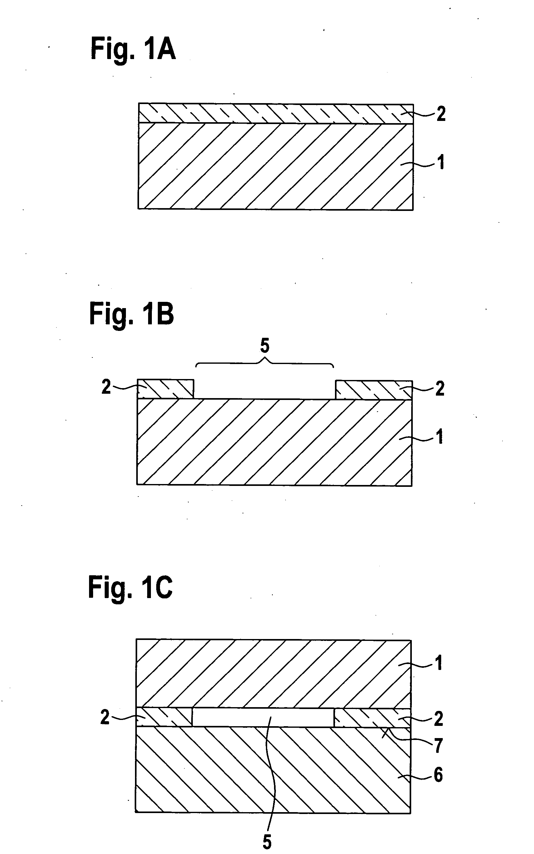
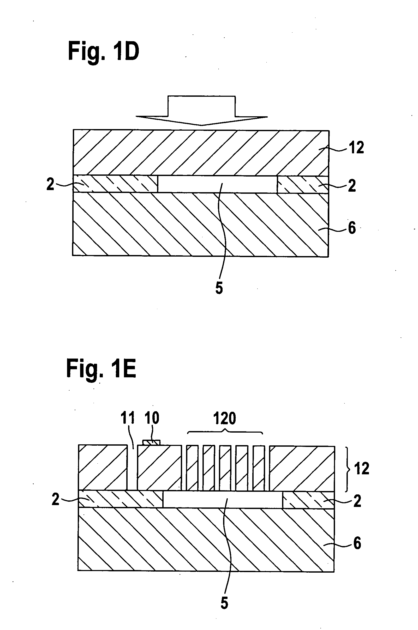
[0042]FIGS. 1A through 1E show the anodic bonding of a base wafer with an intermediate layer and a second wafer. In one embodiment of the method, an SOI wafer is manufactured in this way. FIG. 1A shows a silicon substrate 1 and deposited intermediate layer 2. In an advantageous embodiment of the method according to the present invention, a glass layer 2 is applied as intermediate layer 2 to silicon substrate 1, using a spin-on-glass technique (SOG), and heated, so that a planar surface is obtained on layer 2. As shown in FIG. 1B, layer 2 may be structured by etching, for example, so that recesses 5, which are subsequently located underneath the sensor structure, are obtained. The etching step creates adjustment marks for recesses 5, which may be used for the subsequent adjustment of the back surfaces. Layer 2 may, however, also be processed unstructured. In the following step, ...


PUM


Abstract

A method for anodic bonding of wafers and a device essentially composed of such bonded wafers. An intermediate layer is placed between two wafers, after which the two wafers are anodically bonded. The method and the device have the advantage of being implementable and manufacturable, respectively, in a particularly cost-effective manner. The anodically bonded intermediate layer plastically encloses any possible particles present or evens out differences in height of the wafer surfaces to be bonded and thus prevents any extensive bond defects from occurring.

Description

BACKGROUND INFORMATION [0001] Manufacturing of SOI (silicon on insulator) wafers was originally motivated by the development of microelectronics to achieve better electrical insulating of the integrated circuit against the substrate, for example for high-current or high-temperature applications. A typical SOI wafer which is suitable for processing microelectronic circuits has a base wafer which has a typical thickness between 800 μm and 300 μm. A thin oxide, which has a thickness of approximately 0.5 μm to 2 μm, is applied to the base wafer. A monocrystalline silicon layer having a thickness between 1 μm and 100 μm is situated over the oxide. The crystal quality of the upper silicon layer is important for implementing the integrated circuit elements. [0002] In the past few years, SOI wafers have increasingly aroused the interest of manufacturers of microelectromechanical structures (MEMS). In particular, for applications in the area of optical MEMS components or rotational speed sen...

Claims


Application Information

Patent Timeline
Patent Type & Authority Applications(United States)
IPC IPC(8): H01L21/20H01L21/58H01L21/762
CPCH01L21/2007H01L2924/01068H01L24/26H01L24/83H01L2224/8385H01L2224/83894H01L2924/01005H01L2924/01013H01L2924/0102H01L2924/01057H01L2924/01058H01L2924/01063H01L2924/01079H01L2924/01082H01L2924/07802H01L2924/14H01L2924/01033H01L21/76256B81C1/00357
Inventor FISCHER, FRANKGRAF, ECKHARD
Owner ROBERT BOSCH GMBH
Why Eureka
Try Eureka