Radical assisted oxidation apparatus

a technology of oxidation apparatus and oxidation film, which is applied in the direction of lighting and heating apparatus, muffle furnaces, furnaces, etc., can solve the problems of physical limitation, inability to control the diffusion of impurities, and difficulty in applying film to practical us

Inactive Publication Date: 2005-06-02
ELECTRONICS & TELECOMM RES INST
View PDF3 Cites 275 Cited by
  • Summary
  • Abstract
  • Description
  • Claims
  • Application Information

AI Technical Summary

Benefits of technology

[0018] The present invention is contrived to solve the aforementioned problems. According to a radical assisted oxidation apparatus of the present invention, a plenty of radicals are generated by irradiating a light having a short wavelength such as UV to a reaction gas, and components of the radicals and energy distribution are controlled by supplying the generated radicals to a growth chamber.

Problems solved by technology

However, if the thickness of the gate oxide film becomes thinner as described above, it is impossible to control a diffusion of an impurity from a polycrystalline gate, a tunneling current, an impurity of an interface, and a defect such as a pit or a pipe, thereby reaching a physical limitation.
Generally, a low temperature thermal oxidation process widely in use is carried out in a furnace having a temperature of 700° C., and a rapid thermal oxidation (RTO) process is carried out at a temperature of 900° C. However, since the above thermal oxidation processes are not suitable for manufacturing a device using SiGe, a method for forming a laser oxide film, plasma anodization, electrochemical anodization, a method for forming an ozone oxide film, etc. have been studied.
An oxide film grown by an UV laser or an electrochemical anodization method is porous and a structure thereof is not dense, so that the film has many defects, whereby there has been a difficulty in applying the film to practical use.
However, there have been some problems that GeO2 / SiO2 layer is formed separately, Ge metal is precipitated, and a crystal defect may be generated due to a high-energy ion.
And, it is supposed that there is a limitation in reducing the thickness of the oxide film to 1 nm or less, since an inversion layer having a thickness of about 3 nm is formed in a polycrystalline direction of the gate.
As a result, such a problem still remains that a depletion layer existing at an interface with a channel has a thickness of 0.3 to 0.6 nm, although a metal gate is employed.
However, there still remains a limitation in improving the quality of the oxide film, which has the thickness of several atomic layers.
As an example, there was a prior art in which a radical is employed by decomposing a gas, however, it was not perfect in manufacturing a device having a superior performance.
Meanwhile, if a conventional method for forming an oxide film is applied to a silicon germanium (SiGe), which is employed for a hetero junction quantum device, there is a problem that a germanium (Ge) moves into an interface and a precipitation would be generated (referring to “Effects of Si-cal layer thinning and Ge segregation on the characteristics of Si / SiGe / Si heterostructure pMOSFETs, Solid-State Electronics, 46, 2002, written by Y. J. Song, J. W. Lim, J. Y. Kang, and K. H. Shim).
However, it is difficult to form an insulation film having a high purity due to an implantation of impurities resulting from repeated uses of plasma.
Thus, at present, it cannot be applied to the product.
However, it has demerits that it is difficult to generate the radical uniformly on the wafer and a Si—Si bonding of the surface may be rapidly broken due to a radical having a high energy.
In this case, it is difficult to effectively arrange the UV lamp 17 on the tube 11 or around the tube 11.
In addition, it is difficult to design a metal plate housing having a high reflectance to an optimized structure.
Further, a bonding between atoms may be broken or unstable at the surface of the wafer since a radical or an ion having a high energy is directly irradiated thereto.
Thus, a defect such as a fixed electron may be implanted to the oxide film.
Like the conventional methods, the above method has a problem that a defect may be implanted during forming a thin film since a radical or an ion having a high energy is directly irradiated to the surface.
Therefore, there has been a limitation in forming a dielectric film with a high purity and quality.
In addition, the rapid thermal treatment using the IR lamp would be impossible since the upper electrode and the lower electrode are manufactured with a metal.

Method used


Image

  • Radical assisted oxidation apparatus
  • Radical assisted oxidation apparatus
  • Radical assisted oxidation apparatus

Examples


Embodiment Construction

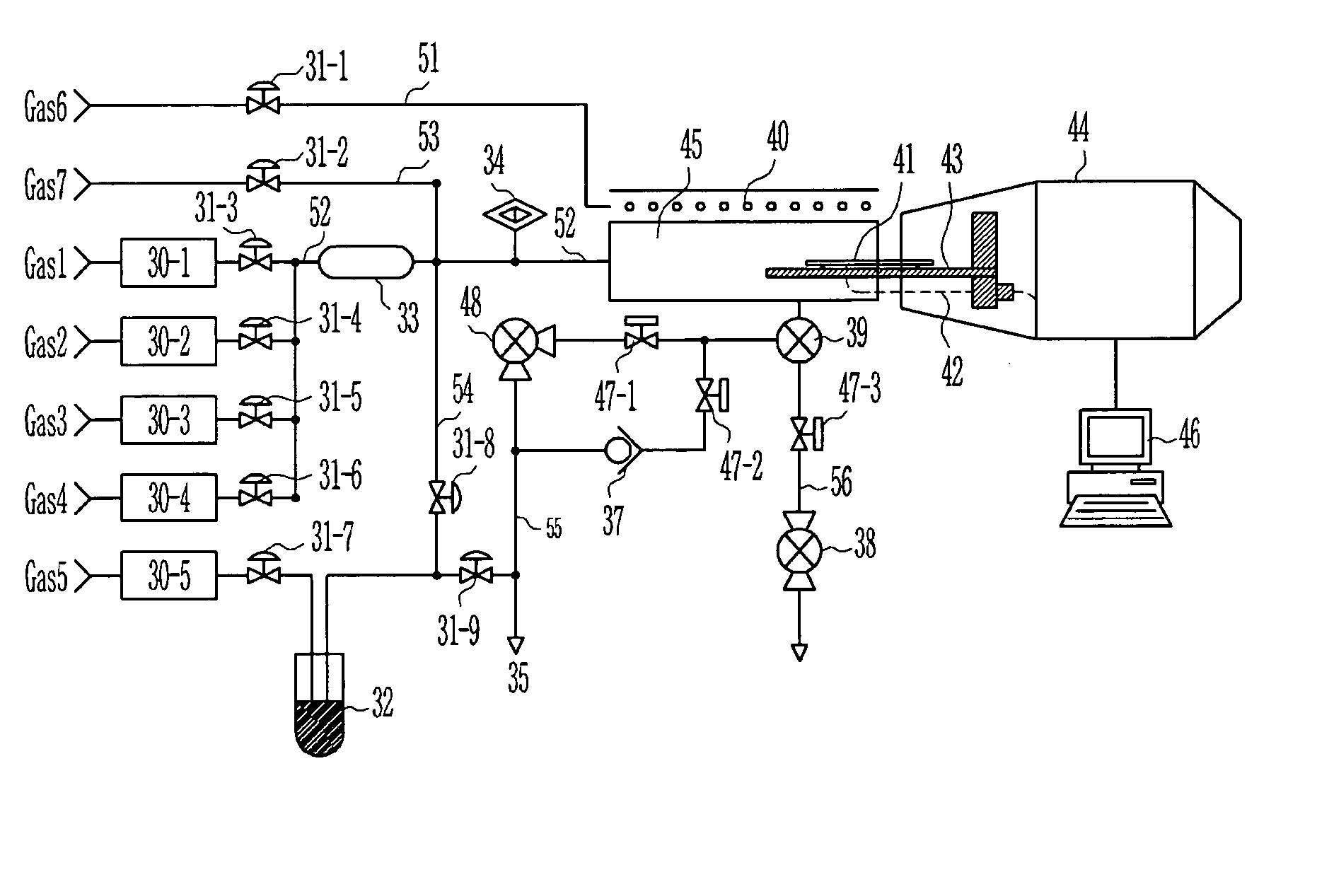
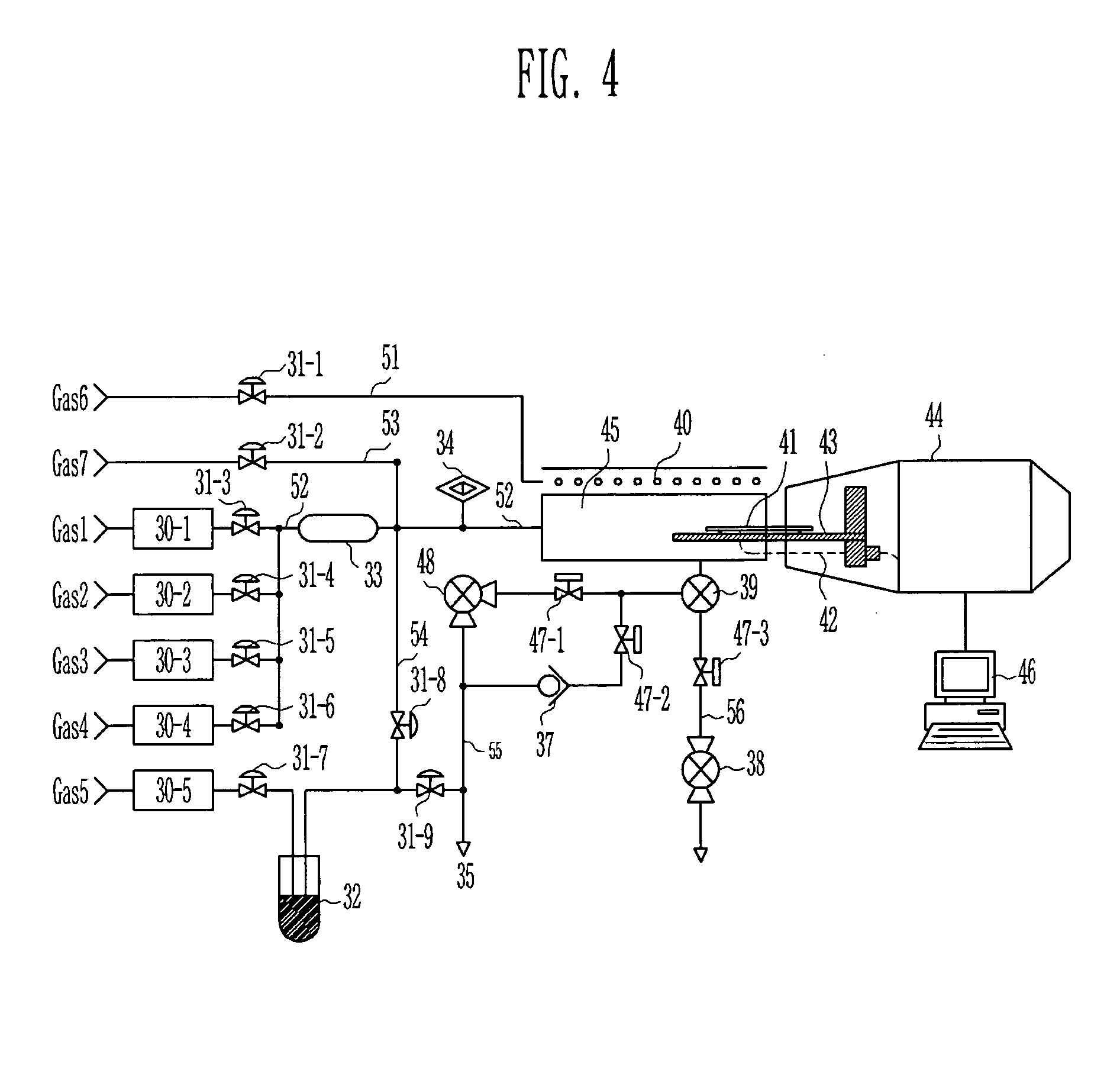
[0034] Now, the preferred embodiments according to the present invention will be described with reference to accompanying drawings. Since preferred embodiments are provided for the purpose that the ordinary skilled in the art are able to understand the present invention, they may be modified in various manners and the scope of the present invention is not limited by the preferred embodiments described later.

[0035] In an integration of a semiconductor device, a primary variable of a scaling factor (1 / α) related to a decrease of a device size may be a gate length and width. Thus, a degree of integrity increases proportional to α2, power consumption decreases proportional to 1α2

since a driving voltage (Vgs−Vth) is controlled to have a small value, and an operation speed would be improved. A drain saturation current in a channel of a device could be represented as follows in Equation 1; ID,sat=WL⁢μ⁢ ⁢Cinv⁢(VGS-Vth)22⁢n〈Equation⁢ ⁢1〉

[0036] Where, n=1+Cd / COX, SS(mV / dec)=n(kT / q)ln(10)....


PUM


Abstract

Provided is a radical assisted oxidation apparatus comprising a gas supply system, a radical source, a growth chamber, a load lock chamber, and a vacuum system, whereby it is possible to manufacture a high quality oxide film at a low temperature and improve a low frequency noise (1/f).

Description

BACKGROUND [0001] 1. Field of the Invention [0002] The present invention relates to an oxidation apparatus for manufacturing a semiconductor device and, more particularly, to a radical assisted oxidation apparatus capable of growing an oxide film with a high quality at a low temperature. [0003] 2. Discussion of Related Art [0004] A process for manufacturing a silicon semiconductor has been developed remarkably owing to a development of a new technology. In particular, a necessity for a CMOS device employing a SiGe has been increased, as markets of a high performance microprocessor and a radio communication are getting broader. In the CMOS device, an operation characteristic of a MOSFET comprising a metal, an oxide, a silicon (Si), etc. depends on a characteristic of a gate dielectric film. The dielectric film is mainly formed with an oxide or a nitride, and a development for process technology has been required to improve an interface characteristic and state of the dielectric film....

Claims


Application Information

Patent Timeline
Patent Type & Authority Applications(United States)
IPC IPC(8): F27B5/14F27B17/00H01L21/205H01L21/00H01L21/316H01L21/44
CPCF27B17/0025H01L21/02126H01L21/02178H01L21/67115H01L21/02255H01L21/02271H01L21/31662H01L21/02236H01L21/205
Inventor SHIM, KYU HWANSONG, YOUNG JOOKIM, SANG HOONLEE, NAE EUNGKANG, JIN YEONG
Owner ELECTRONICS & TELECOMM RES INST
Why Eureka
Try Eureka