Stacked chip semiconductor device

a semiconductor device and stacked chip technology, applied in semiconductor devices, semiconductor/solid-state device details, electrical equipment, etc., can solve the problems of low area efficiency of chip layout, difficult to miniaturize device may not be cost-effective, so as to reduce power consumption of stacked chip semiconductor devices, the effect of miniaturization of electronic systems and reducing power consumption

Active Publication Date: 2005-06-02
RENESAS ELECTRONICS CORP
View PDF13 Cites 29 Cited by
  • Summary
  • Abstract
  • Description
  • Claims
  • Application Information

AI Technical Summary

Benefits of technology

[0018] (1) A compact stacked chip semiconductor device is realized.
[0019] (2) Power consumption of a stacked chip semiconductor device is reduced.
[0020] (3) The above effects (1) and (2) contribute to miniaturization of electronic systems and reduction in their power consumption.

Problems solved by technology

However, the inventors have found that the above stacked chip semiconductor device has the following problems.
Although the address terminals and data input / output terminals are shared as mentioned above, the area efficiency in chip layout is low because each semiconductor chip has a function of interfacing with an externally connected module.
As a consequence, it may be difficult to miniaturize the stacked chip semiconductor device and also the device may be not cost-effective.

Method used


Image

  • Stacked chip semiconductor device
  • Stacked chip semiconductor device
  • Stacked chip semiconductor device

Examples


first embodiment

[0035]FIG. 1 is a top view of a stacked chip semiconductor device according to a first embodiment of the present invention, FIG. 2 is a sectional view of the stacked chip semiconductor device of FIG. 1, FIG. 3 illustrates an interface circuit in the stacked chip semiconductor device of FIG. 1, FIG. 4 is a circuit diagram of an ESD protection circuit and an input buffer which are incorporated in the interface circuit of FIG. 3, and FIG. 5 is a circuit diagram of an output buffer incorporated in the interface circuit of FIG. 3.

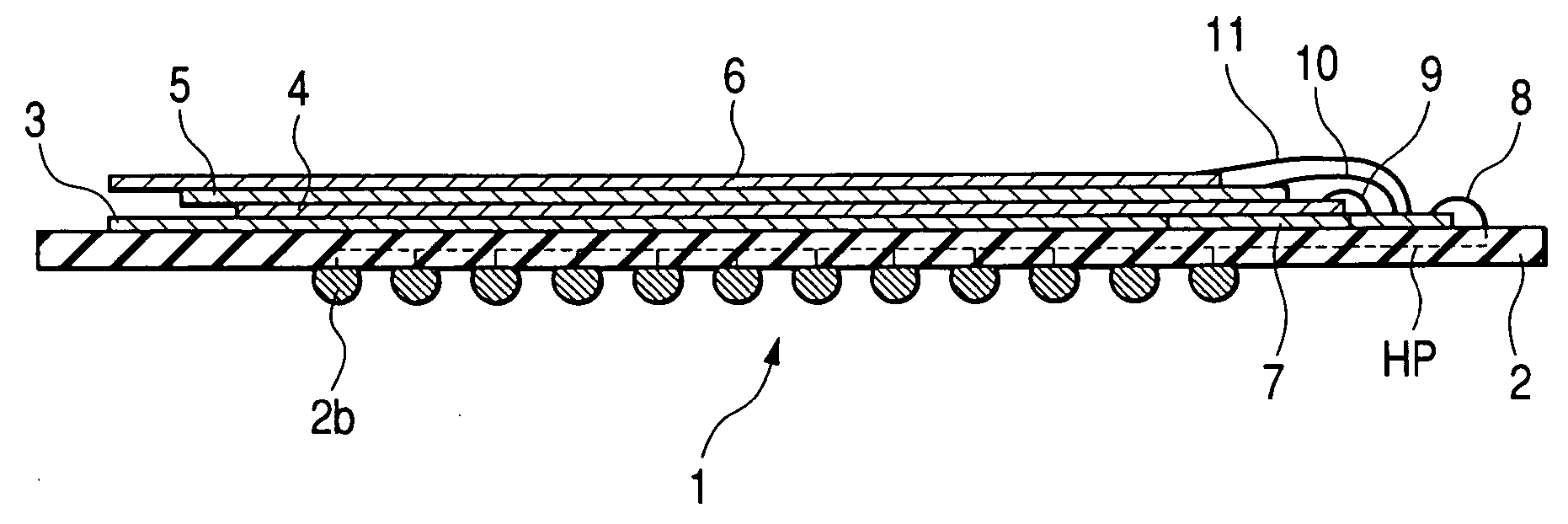
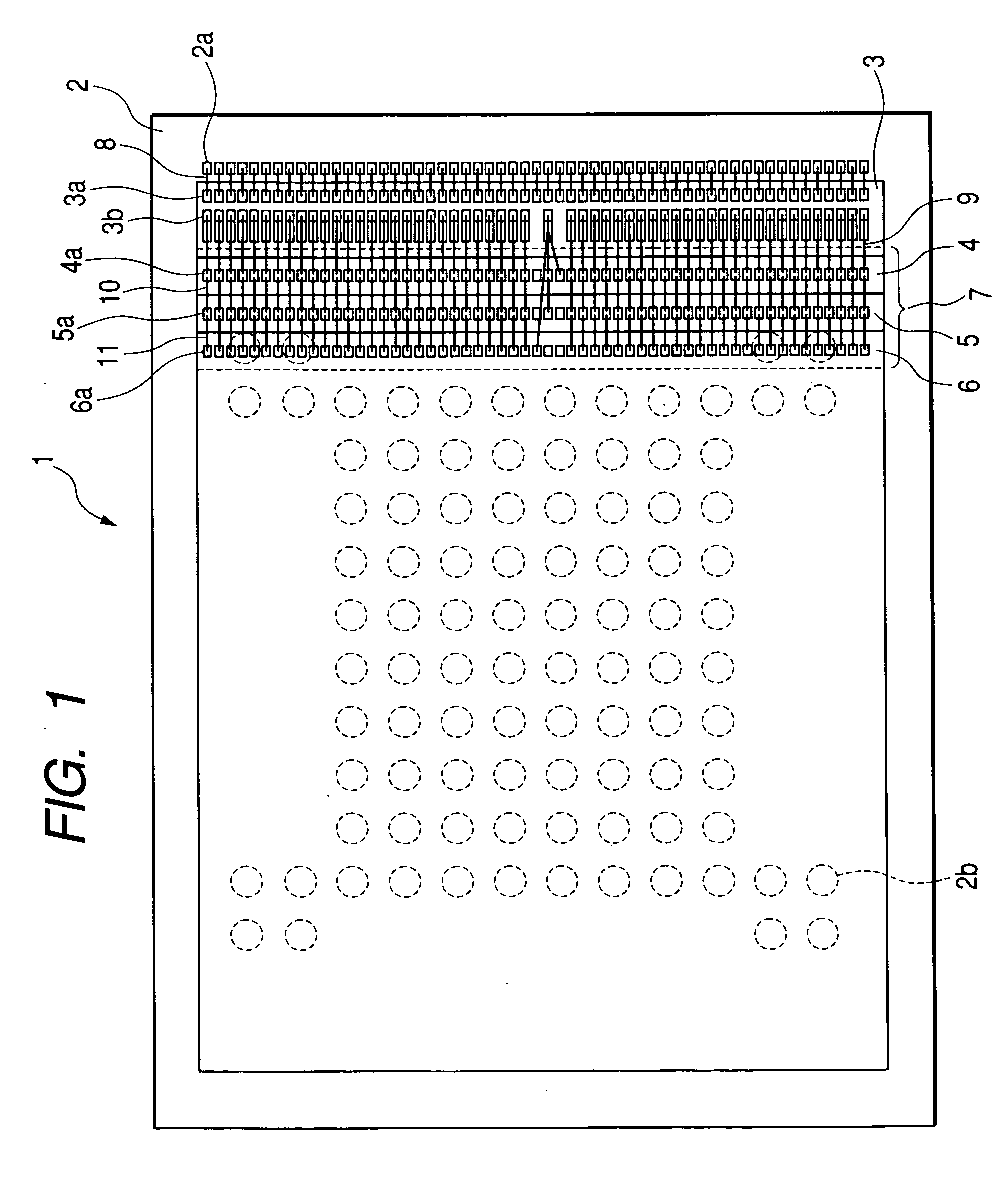
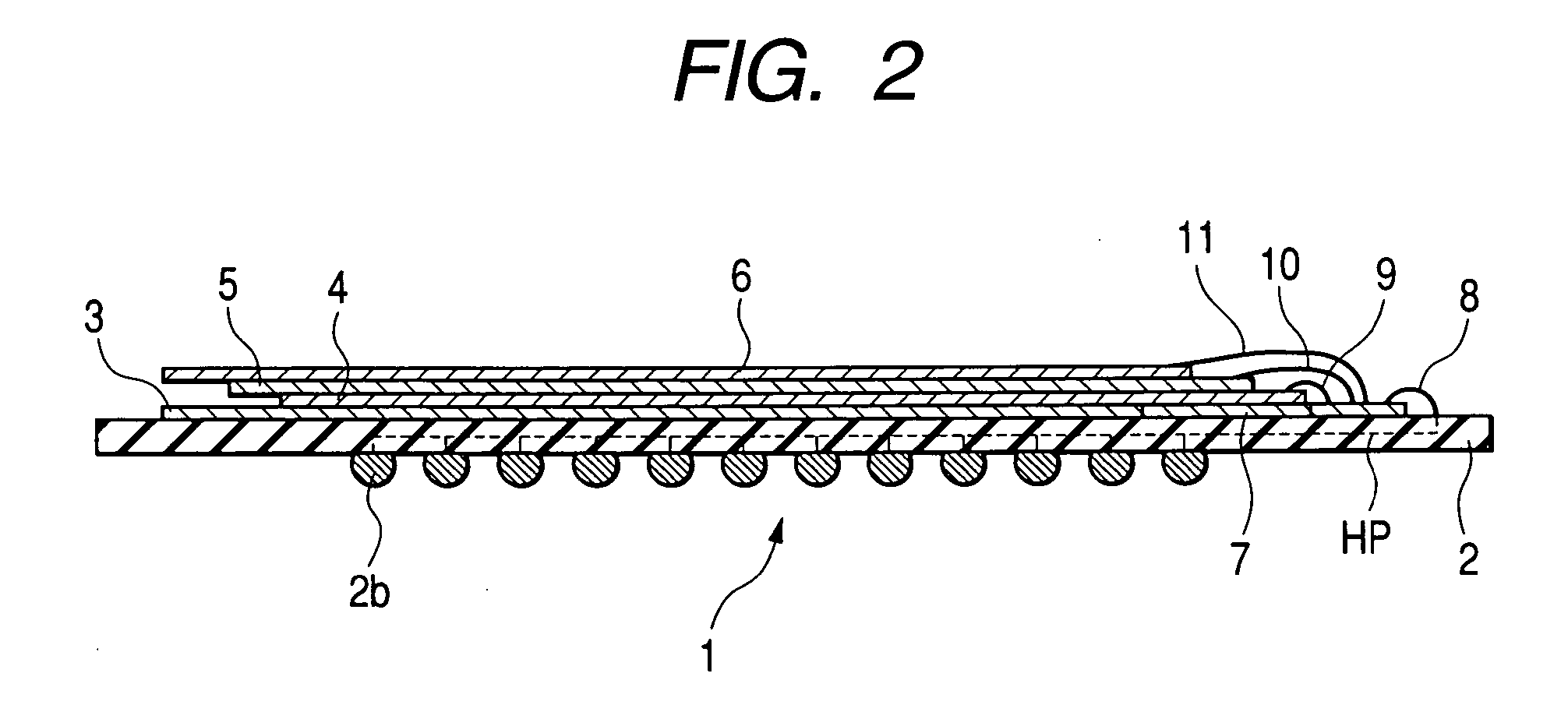
[0036] In the first embodiment, a stacked chip semiconductor device 1 consists of a BGA (Ball Grid Array) as a kind of surface mount CSP. As shown in FIGS. 1 and 2, the semiconductor device 1 has a printed wiring board 2, for example, made of BT (Bismaleimide Triazine). On the back of the printed wiring board 2 is an array of electrodes for connection.

[0037] The printed wiring board 2 has a stacked structure in which semiconductor chips 3 to 6 are stacked in t...

second embodiment

[0080]FIG. 7 is a top view of a stacked chip semiconductor device according to the second embodiment of the present invention; and FIG. 8 is a sectional view of the stacked chip semiconductor device of FIG. 7.

[0081] As shown in FIGS. 7 and 8, in the second embodiment, the stacked chip semiconductor device 1b consists of a BGA with a stacked structure. Like the first embodiment (see FIGS. 1 and 2), the stacked chip semiconductor device 1b includes a printed wiring board 2, solder bumps 2b, semiconductor chips 3 to 6, bonding wires 8a and bonding wires 9 to 11. The difference from the first embodiment is the layout of the interface circuit of the semiconductor chip 3.

[0082] The interface circuit 7 is located not on the periphery of the external connection electrodes 3a and internal connection electrodes 3b on the semiconductor chip 3, but on the side facing the side where the external connection electrodes 3a are located.

[0083] The connection electrodes are located on the back surf...

third embodiment

[0090]FIG. 9 is a sectional view of a stacked chip semiconductor device according to the third embodiment of the present invention.

[0091] In the third embodiment, a stacked chip semiconductor device 1c is the same as in the first embodiment except that a semiconductor chip (semiconductor chip with ESD protection) 27 is newly added and semiconductor chips 31, and 4 to 6 only have memory sections.

[0092] As shown in FIG. 9, in the stacked chip semiconductor device 1c, the connection electrodes are located on the back surface of the printed wiring board 2 as an array. The semiconductor chips 31, and4 to 6 are stacked in the center of the main surface of the printed wiring board 2 and the additional semiconductor chip 27, on which an interface circuit 7 (FIG. 3) is structured, lies over the semiconductor chip 6.

[0093] The bonding electrodes 2a are located on the right side of the periphery of the main surface of the printed wiring board 2. The bonding electrodes 2a are electrically co...


PUM


Abstract

A stacked chip semiconductor device whose size is substantially reduced by high density packaging of two or more semiconductor chips. In the semiconductor device, four semiconductor chips are stacked over a printed wiring board. The bottom semiconductor chip has an interface circuit which includes a buffer and an electrostatic discharge protection circuit. All signals that these semiconductor chips receive and send are inputted or outputted through the interface circuit of the bottom semiconductor chip. Since the other semiconductor chips require no interface circuit, the semiconductor device is compact.

Description

CROSS-REFERENCE TO RELATED APPLICATION [0001] The present application claims priority from Japanese patent application No. 2003-398469 filed on Nov. 28, 2003, the content of which is hereby incorporated by reference into this application. BACKGROUND OF THE INVENTION [0002] The present invention relates to technology for miniaturization of semiconductor integrated circuit devices and more particularly to technology, which is effective for stacked chip semiconductor devices in which two or more semiconductor chips are stacked. [0003] With the recent trend toward smaller and higher-performance electronic systems, demand for smaller and higher-density semiconductor integrated circuit devices is growing. One widely-known technique for increasing the density of a package almost equal in size to a semiconductor chip is a semiconductor device with two or more semiconductor chips stacked which is called a stacked CSP (Chip Size Package). [0004] In this stacked chip semiconductor device, two ...

Claims


Application Information

Patent Timeline
Patent Type & Authority Applications(United States)
IPC IPC(8): H01L23/60H01L25/065
CPCH01L23/60H01L2924/13091H01L2224/48091H01L2224/48145H01L2224/48227H01L2224/49175H01L2225/06562H01L2924/15311H01L2924/3011H01L25/0657H01L2924/1301H01L2224/73265H01L2224/32225H01L2224/32145H01L24/49H01L24/48H01L2924/00014H01L2924/00H01L2924/00012H01L24/73H01L2924/14H01L2224/05554H01L2224/45099H01L2224/45015H01L2924/207
Inventor TSUNOZAKI, MANABU
Owner RENESAS ELECTRONICS CORP
Why Eureka
Try Eureka