
High density contact to relaxed geometry layers

a geometry layer and high density technology, applied in the direction of semiconductor devices, semiconductor/solid-state device details, electrical equipment, etc., can solve the problems of inefficient space utilization and extra processing steps of conventional arrangemen

Active Publication Date: 2005-06-16
SANDISK TECH LLC
View PDF16 Cites 43 Cited by
  • Summary
  • Abstract
  • Description
  • Claims
  • Application Information

AI Technical Summary

Problems solved by technology

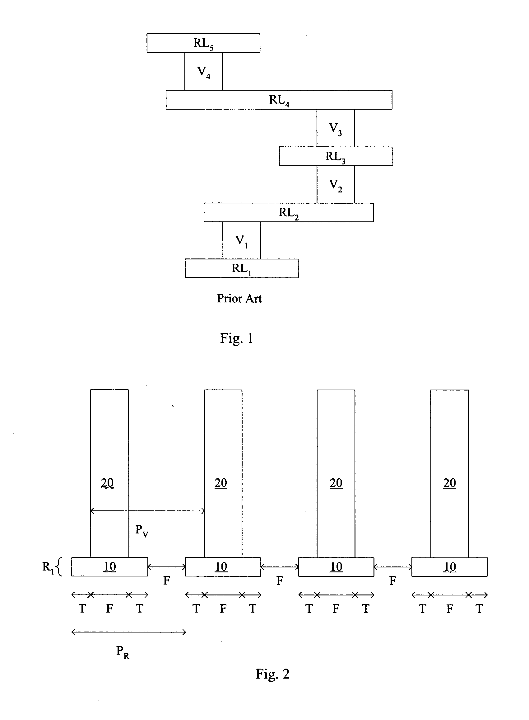
With the advent of extremely dense structures requiring extensive interconnection, including, for example, interconnection between layers that are not vertically adjacent, while the highest possible density must be maintained, this conventional arrangement uses space inefficiently and requires extra processing steps.

Method used


Image

  • High density contact to relaxed geometry layers
  • High density contact to relaxed geometry layers
  • High density contact to relaxed geometry layers

Examples


Embodiment Construction

[0024] Monolithic three dimensional memory arrays are described in Johnson et al., U.S. Pat. No. 6,034,882, “Vertically stacked field programmable nonvolatile memory and method of fabrication”; Johnson, U.S. Pat. No. 6,525,953, “Vertically stacked field programmable nonvolatile memory and method of fabrication”; Knall et al., U.S. Pat. No. 6,420,215, “Three Dimensional Memory Array and Method of Fabrication”; Lee et al., U.S. patent application Ser. No. 09 / 927648, “Dense Arrays and Charge Storage Devices, and Methods for Making Same,” filed Aug. 13, 2001; Herner, U.S. application Ser. No. 10 / 095962, “Silicide-Silicon Oxide-Semiconductor Antifuse Device and Method of Making,” filed Mar. 13, 2002; Vyvoda et al., U.S. patent application Ser. No. 10 / 185507, “Electrically Isolated Pillars in Active Devices,” filed Jun. 27, 2002; Herner et al., U.S. patent application Ser. No. 10 / 326470, “An Improved Method for Making High Density Nonvolatile Memory,” filed Dec. 19, 2002; Walker et al., U...


PUM


Abstract

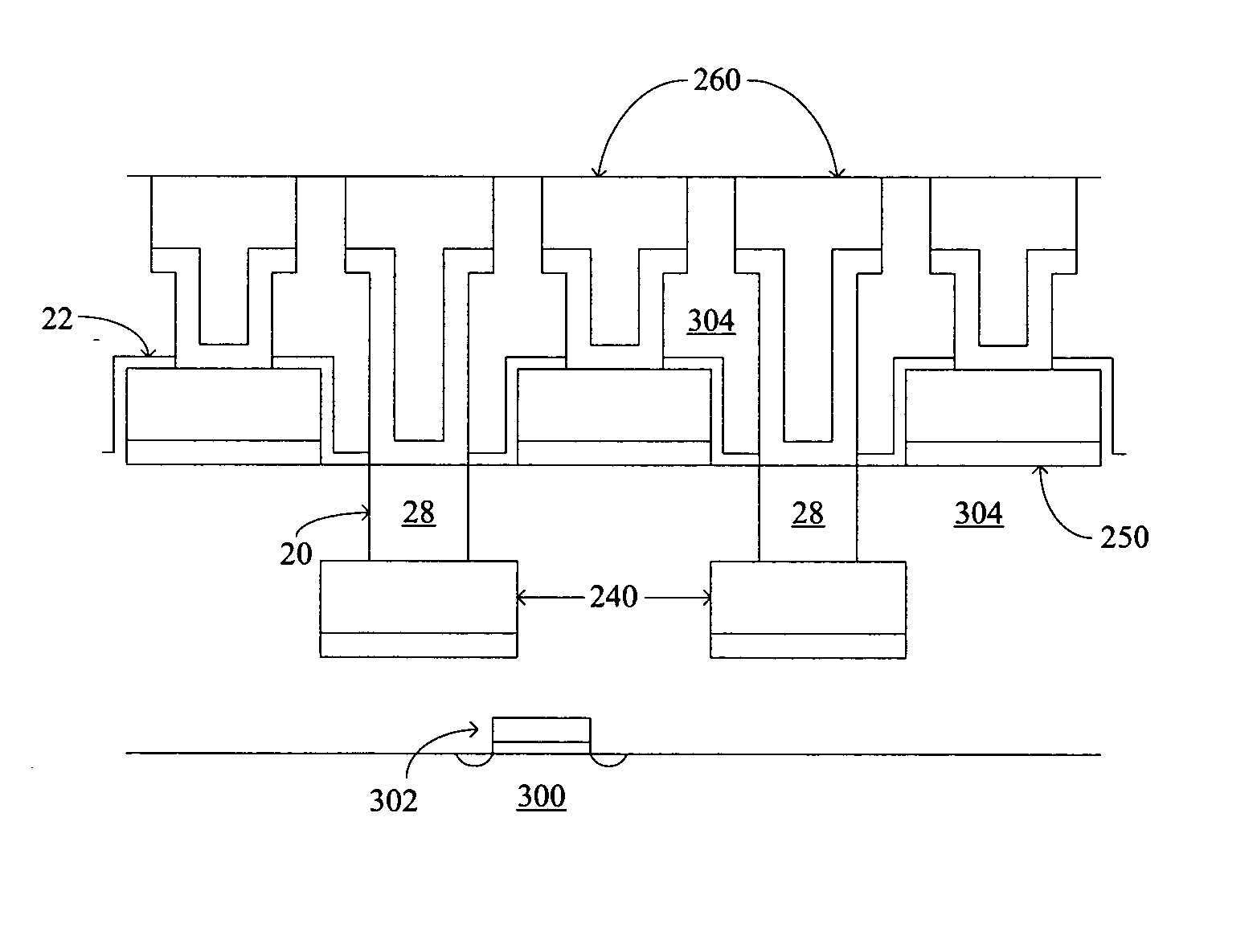
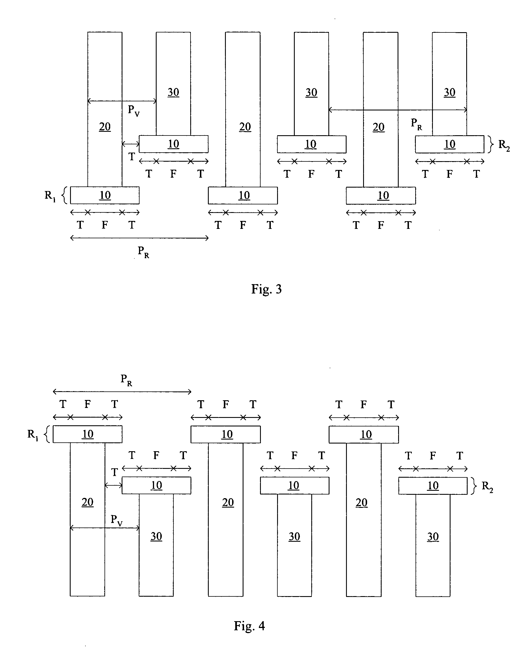
The present invention provides for a via and staggered routing level structure. Vertically overlapping vias connect to two or more routing levels formed at different heights. The routing levels are either both formed above or both formed below the vias, and all are formed above a semiconductor substrate wafer. In this way vias can be formed having a pitch smaller than the pitch of either the first routing level or the second routing level, saving space.

Description

RELATED APPLICATIONS [0001] This application is related to Cleeves et al., U.S. application Ser. No. ______, “Optimization of Critical Dimensions and Pitch of Patterned Features in and Above a Substrate,” (attorney docket no. MA-110) filed on even date herewith, which application is hereby incorporated by reference.BACKGROUND OF THE INVENTION [0002] The invention relates to a structure for providing electrical interconnection between levels formed at different heights in an integrated circuit, specifically to elements in a dense multilevel array. [0003] It is known to form vias to electrically connect routing levels formed at different heights in an integrated circuit. In a conventional arrangement, shown in FIG. 1, bottom routing level RL1 is formed first. Generally a dielectric material is deposited on RL1. The dielectric material is selectively excavated to form a hole, which is then filled with a conductive material to form via V1. In the same manner routing level RL2 is formed ...

Claims


Application Information

Patent Timeline
IPC IPC(8): H01L21/8246H01L21/8247H01L23/522H01L27/115H01L29/40
CPCH01L23/5226H01L27/11568H01L27/11521H01L27/115H01L2924/0002H01L23/522H01L23/5283H10B43/30H10B69/00H10B41/30H01L2924/00
Inventor SCHEUERLEIN, ROY E.PETTI, CHRISTOPHER J.
Owner SANDISK TECH LLC
Learn More