Test pad array for contact resistance measuring of ACF bonds on a liquid crystal display panel

a liquid crystal display panel and test pad array technology, applied in the field of anisotropic conductive film contact resistance measurement on an lcd panel, can solve the problem of not having a convenient method for measuring the contact resistance of acf bonds directly on the lcd panel

Active Publication Date: 2005-06-16
AU OPTRONICS CORP
View PDF8 Cites 28 Cited by
  • Summary
  • Abstract
  • Description
  • Claims
  • Application Information

AI Technical Summary

Benefits of technology

[0004] A test pad array is disclosed for measuring anisotropic conductive film bond contact resistance on a liquid crystal display panel. The test pad array is provided on a surface of the liquid crystal display panel. The test pad array is electrically connected to a group of terminal pads disposed on the surface of the panel, which are electrically connected to an electronic device with anisotropic conductive film bonds. The test pad array allows the contact resistance of one or more of the anisotropic conductive film bonds to be measured on the panel.

Problems solved by technology

Presently, however, there is no convenient method for measuring the contact resistance of the ACF bonds directly on the LCD panels.

Method used


Image

  • Test pad array for contact resistance measuring of ACF bonds on a liquid crystal display panel
  • Test pad array for contact resistance measuring of ACF bonds on a liquid crystal display panel
  • Test pad array for contact resistance measuring of ACF bonds on a liquid crystal display panel

Examples


Embodiment Construction

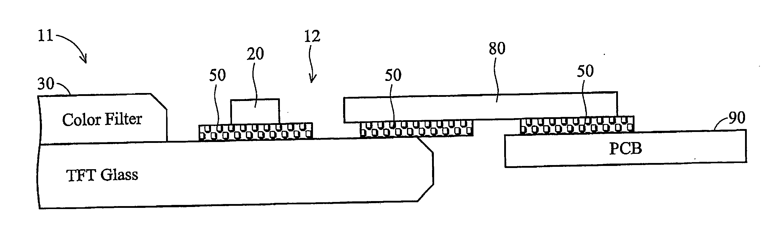
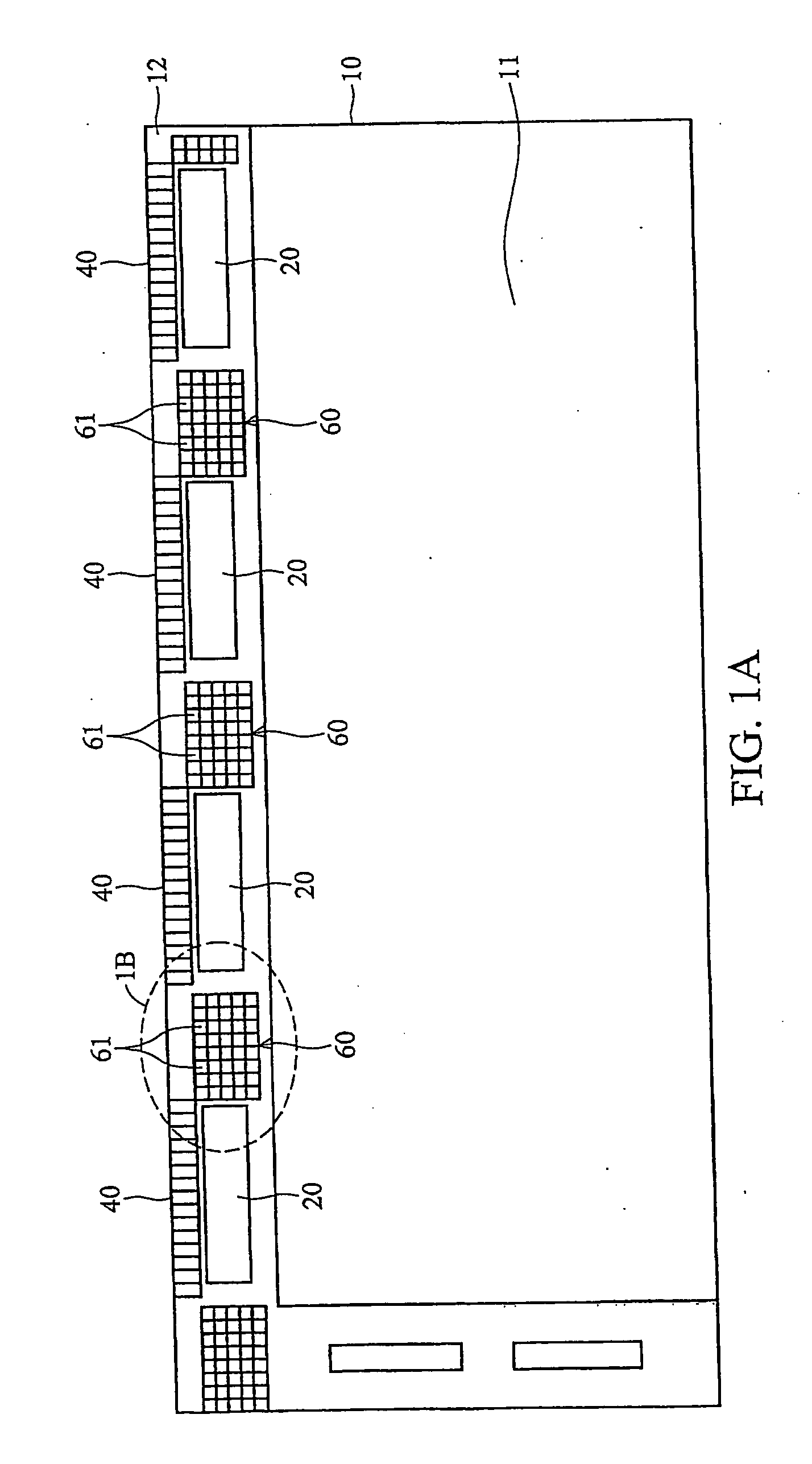
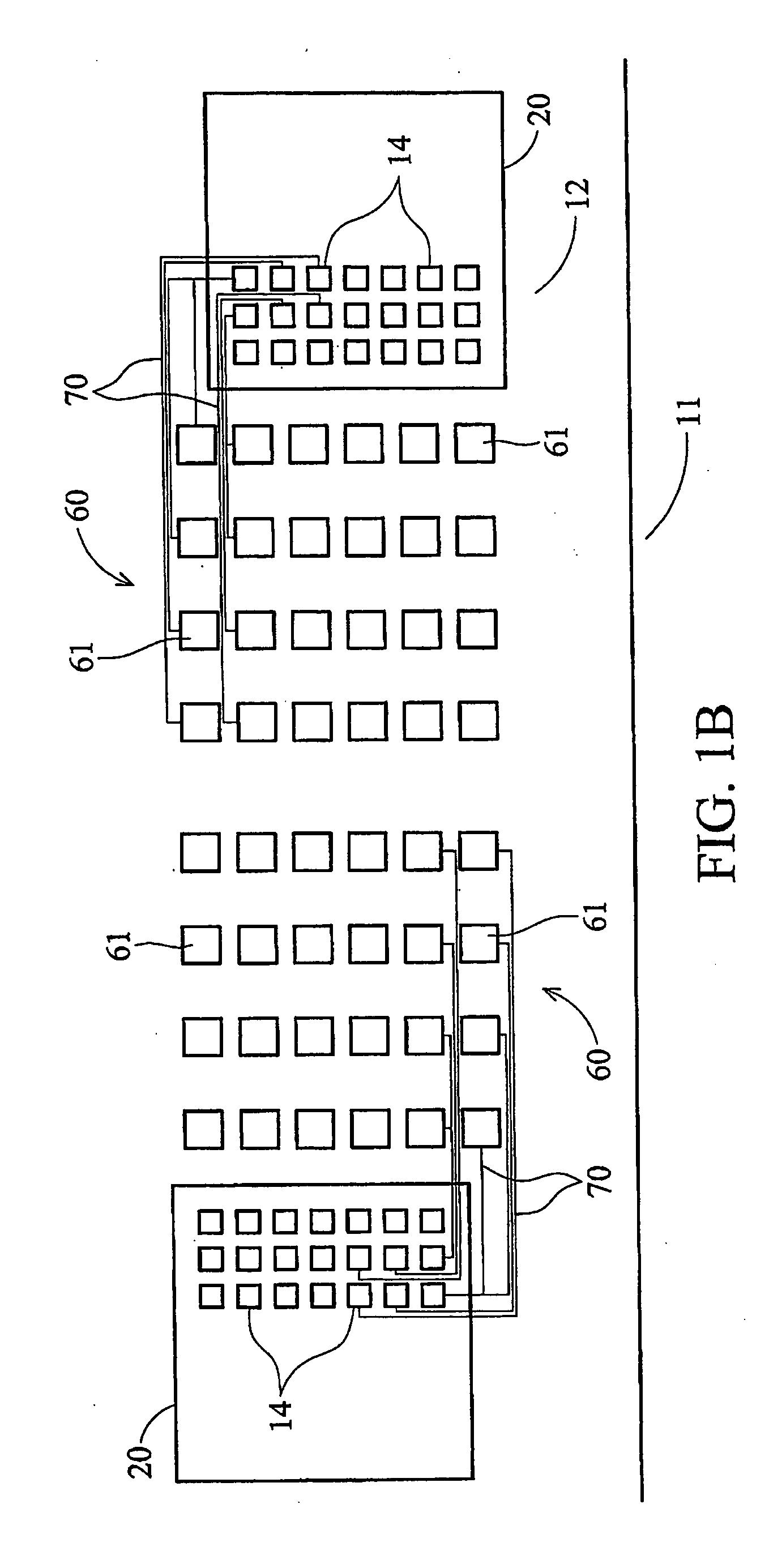
[0015] The present invention is a test pad array for contact resistance measuring of anisotropic conductive film (ACF) bonds, on a liquid-crystal-display (LCD) panel. The contact resistance measurements can be used for archiving different bonding process conditions. The test pad array also allows for electronic character testing and improves ACF adhesion to the panel after the test pad array has been utilized to perform resistance and character testing.

[0016]FIG. 1A is a plan view of an illustrative embodiment of an LCD panel 10 with chip-on-glass (COG) bonded driver integrated circuit chips (ICs) 20. The panel 10, which may be made from glass or quartz substrate, includes a pixel region 11 and a peripheral region 12. The pixel region 11 includes a pixel thin film transistor (TFT) array and electrically conductive gate and data lines connected to the TFT array. The design of the pixel TFT array and the gate and data lines is well known to persons of ordinary skill in the art and ne...


PUM


Abstract

A test pad array and dummy lead array for measuring anisotropic conductive film bond contact resistance on a liquid crystal display panel. The test pad and dummy lead arrays are provided on a surface of the liquid crystal display panel. The test pad array is electrically connected to a group of terminal pads disposed on the surface of the panel, which are electrically connected to an electronic device with anisotropic conductive film bonds. The test pad array allows the contact resistance of one or more of the anisotropic conductive film bonds to be measured on the panel. The dummy lead array is provided for electrically connecting a second electronic device to the panel. The dummy lead array is electrically connected to the test pad array such that a contact resistance of at least one anisotropic conductive film bond associated with the second electronic device can be measured on the panel using portions of the test pad array electrically connected to the dummy lead array.

Description

FIELD OF THE INVENTION [0001] This invention relates to liquid crystal display (LCD) panels. More particularly, this invention relates to anisotropic conductive film contact resistance measuring on an LCD panel. BACKGROUND OF THE INVENTION [0002] Flat panel display devices commonly use LCD panels. An LCD panel may include a pixel region having an array of pixel thin film transistors and intersecting arrays of spaced apart data lines and gate lines that are connected to the array of pixel thin film transistors. The array of pixel thin film transistors, data lines and gate lines form an array of addressable pixels. The LCD panel may also include a peripheral region associated with driver integrated circuit chips (ICs), which drive the array of pixel thin film transistors. The ICs may be mounted to the LCD panel in the peripheral region thereof using a chip-on-glass (COG), a tape-carrier-package (TCP) or a chip-on-film (COF) technology. In COG, TCP, and COF, anisotropic conductive film...

Claims


Application Information

Patent Timeline
Patent Type & Authority Applications(United States)
IPC IPC(8): G01R27/02G01R31/28G01R27/20G01R31/00G01R31/04G01R31/26G09G3/00H01L21/60
CPCG01R27/205G01R31/046G09G3/006H01L2924/0002H01L2924/00G01R31/70
Inventor CHEN, HUI-CHANG
Owner AU OPTRONICS CORP
Why Eureka
Try Eureka