Ferroelectric memory and data reading method for same

Inactive Publication Date: 2005-06-16
FUJITSU SEMICON LTD
View PDF5 Cites 20 Cited by
  • Summary
  • Abstract
  • Description
  • Claims
  • Application Information

AI Technical Summary

Benefits of technology

[0024] Since the gate voltage of the first pMOS transistor is set at a value that is slightly smaller than its own threshold voltage, a current always leaks from the bit line to the first node to increase the potential of the first node during a read operation. Therefore, for example, a control circuit (a feedback circuit such as an inverter amplifier) for keeping the potential of the bit line at the ground potential during a read operation is not necessary. This makes it possible to decrease the layout size of the ferroelectric memory. Since no such control circuit is necessary, the power consumption of the ferroelectric memory can be reduced.
[0025] According to another aspect of the invention, a second pMOS transistor is turned on by a voltage of a second node and connects the first node to a ground line. Charge is extracted from the second node by a second coupling capacitor before reading of the data from the memory cell, whereby the potential of the second node is temporarily set at a deep negative voltage. Charge is supplied to the second node by a clamping circuit for setting the potential of the second node at a constant voltage, in a period when the potential of the second node is set at the deep negative voltage. The second pMOS transistor is turned on to initialize the first node to the ground potential, in an undershoot period when the potential of the second node varies from the deep negative voltage to the constant voltage. Then, charge is extracted from the first node by a first coupling capacitor to set the potential of the first node at the prescribed negative voltage. Since the potential of the first node can be initialized to the ground potential merely by turning on the second pMOS transistor utilizing the fact that the potential of the second node becomes a deep negative voltage temporarily, the first node can be initialized at high speed. Therefore, the initialization period (precharging period) before a read operation can be shortened and hence the read access time can be shortened. Since the potential of the first node can be initialized by utilizing the circuit for keeping the second node at the constant voltage, circuits necessary for the initialization before a read operation can be simplified in configuration. As a result, the size of the ferroelectric mem

Problems solved by technology

And the long precharging period is an obstru

Method used


Image

  • Ferroelectric memory and data reading method for same
  • Ferroelectric memory and data reading method for same
  • Ferroelectric memory and data reading method for same

Examples


first embodiment

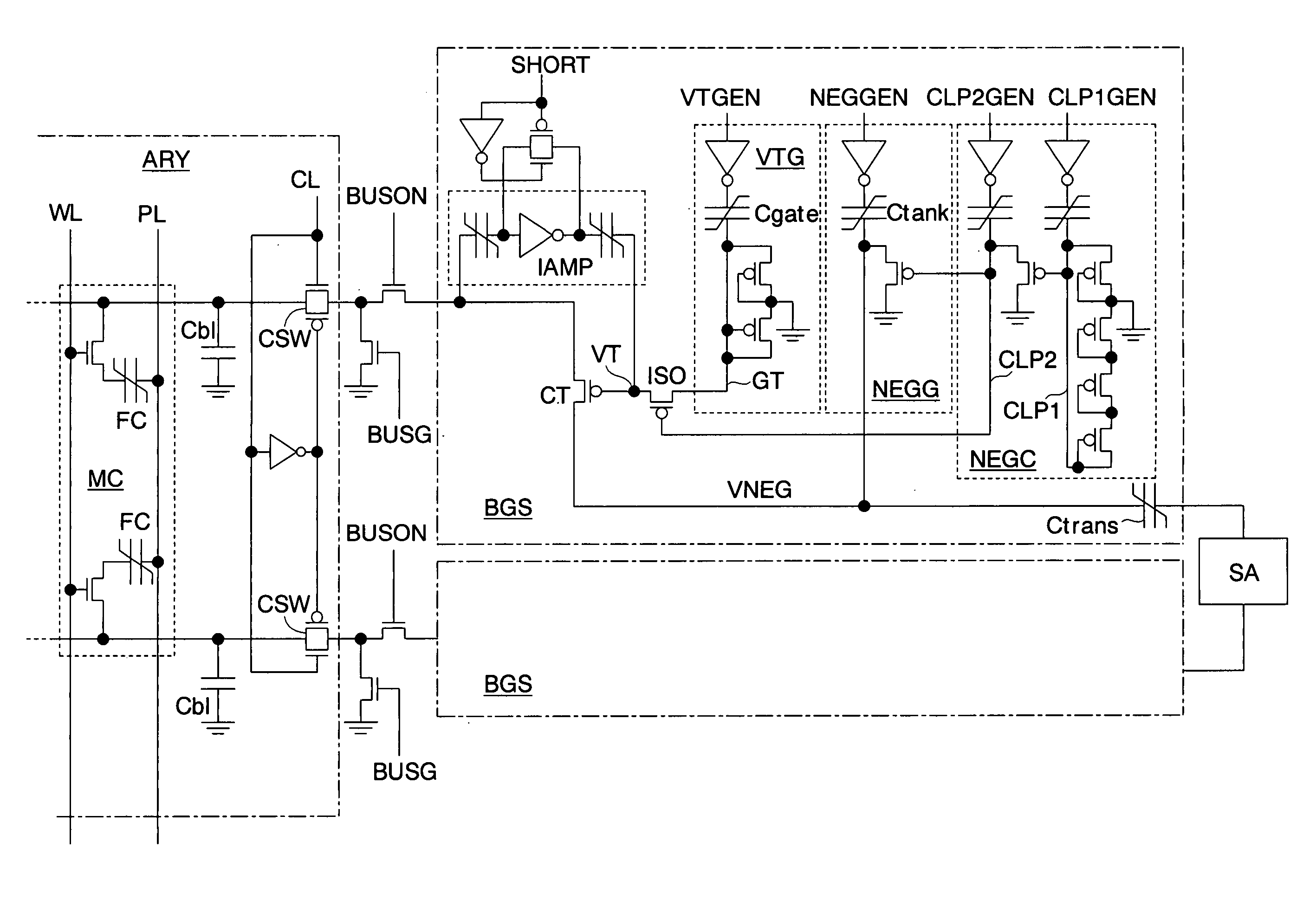
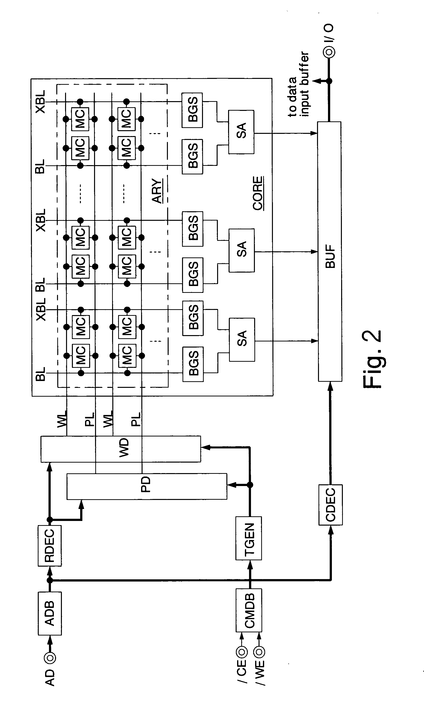
[0040]FIG. 2 shows a ferroelectric memory according to the invention. A ferroelectric memory chip is formed on a silicon substrate by using a CMOS process.

[0041] For example, the ferroelectric memory is used as a work memory of a hand-held terminal such as a cellular phone. The ferroelectric memory has an address buffer ADB, a command buffer CMDB, a row decoder RDEC, a timing generator TGEN, a column decoder CDEC, a plate driver PD, a word driver WD, a memory core CORE, and a data output buffer BUF. FIG. 2 mainly shows circuits that are necessary for a read operation. Therefore, circuits necessary for a write operation such as a data input buffer and a write amplifier are omitted.

[0042] The address buffer ADB receives an address signal via an address terminal and outputs the received signal to the row decoder RDEC and the column decoder CDEC. The row decoder RDEC generates a row decoded signal by decoding upper bits (row address) of the address signal and outputs the generated sign...

second embodiment

[0100]FIG. 9 shows a read operation of the Waveforms shown in the top part of FIG. 9 are input signals and waveforms shown in the bottom part of FIG. 9 are simulation results.

[0101] The timing relationships between the input signals are the same as in the first embodiment. As for the simulation waveforms, the voltages of the nodes SF and XSF are slightly different than in the first embodiment, which results from the difference in the cell structure (1T1C or 2T2C). Symbols with “ref” at the tail denote waveforms of nodes corresponding to the reference memory cell RMC. The voltage of a node that is denoted by a symbol with “ref” is equal to the middle value between the voltages of the associated nodes that are denoted by symbols with “1” and “0,” respectively. As is apparent from FIG. 9, the simulation waveforms are basically the same as in the first embodiment.

[0102] This embodiment can provide the same advantages as the first embodiment does.

[0103] Although the above embodiments ...


PUM


Abstract

A bit line is connected, via a first pMOS transistor, to a first node whose potential is set at a prescribed negative voltage in advance. The gate voltage of the first pMOS transistor is set at a constant voltage that is slightly lower than its threshold voltage. During a read operation, a current that flows into the bit line from a memory cell in accordance with a residual dielectric polarization value of a ferroelectric capacitor always leaks to the first node, whereby the potential of the first node increases. The logical value of data stored in the memory cell is judged on the basis of a voltage increase at the first node. Since no control circuit for keeping the potential of the first node at the ground potential during a read operation is necessary, the layout size and the power consumption of a ferroelectric memory can be decreased.

Description

CROSS-REFERENCE TO RELATED APPLICATION [0001] This application is a continuation application of International Application No. PCT / JP03 / 04559, filed Apr. 10, 2003, and designating the U.S. BACKGROUND OF THE INVENTION [0002] 1. Field of the Invention [0003] The present invention relates to a ferroelectric memory and, more particularly, to a data read circuit for reading out data that were written to ferroelectric capacitors. [0004] 2. Description of the Related Art [0005] Recently, a ferroelectric memory reading method called “bitline GND sensing method” has been proposed (IEEE Journal of Solid-State Circuits, Vol. 37, No. 5, pp. 592-597, May 2002 and Japanese Unexamined Patent Application Publication No. 2002-133857). [0006]FIG. 1 shows the main part of a ferroelectric memory that employs the conventional bit-line GND sensing method. A memory cell array ARY has memory cells MC called “2T2C cells” and column switches CSW. To hold 1-bit information, each 2T2C cell is composed of two tr...

Claims


Application Information

Patent Timeline
IPC IPC(8): G11C11/22
CPCG11C11/22
Inventor KAWASHIMA, SHOICHIROENDO, TORUHIRAYAMA, TOMOHISA
Owner FUJITSU SEMICON LTD
Why Eureka
Try Eureka