Method of surface pretreatment before selective epitaxial growth

a technology of selective epitaxial growth and surface pretreatment, which is applied in the direction of crystal growth process, chemically reactive gas, chemistry apparatus and processes, etc., can solve the problems of rough surface of epitaxial layer, serious undercutting of first sidewall spacer, and junction leakage, and achieve good quality and effective removal of native oxide

Inactive Publication Date: 2005-06-16
UNITED MICROELECTRONICS CORP
View PDF10 Cites 32 Cited by
  • Summary
  • Abstract
  • Description
  • Claims
  • Application Information

AI Technical Summary

Benefits of technology

[0012] The present dry etching process can effectively remove native oxide on the semiconductor substrate, and hence p

Problems solved by technology

However, when a silicide is formed on the source/drain region, the silicide easily contacts with the shallow junction to make junction leakage.
However, as shown in FIG. 1B, the surface pretreatment with strong acid leads to serious undercut

Method used


Image

  • Method of surface pretreatment before selective epitaxial growth
  • Method of surface pretreatment before selective epitaxial growth
  • Method of surface pretreatment before selective epitaxial growth

Examples


Embodiment Construction

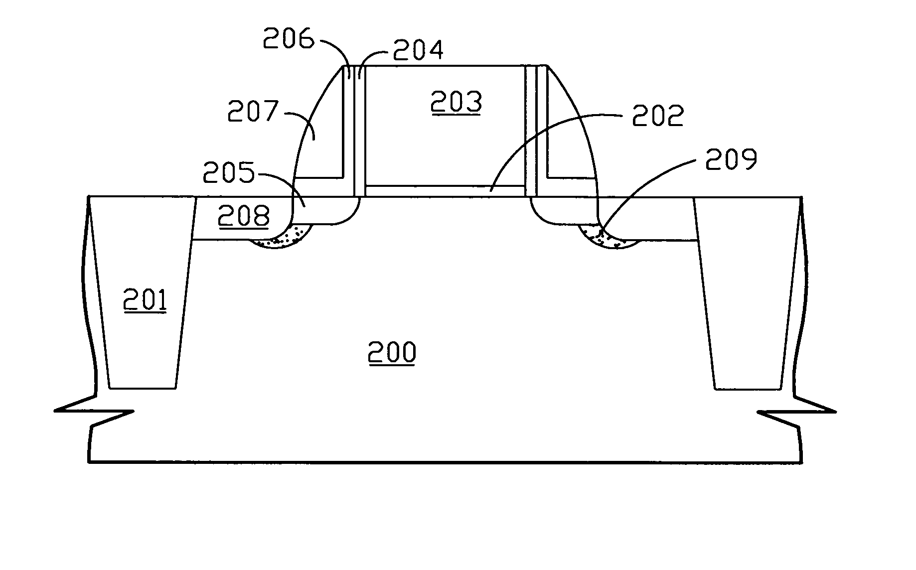
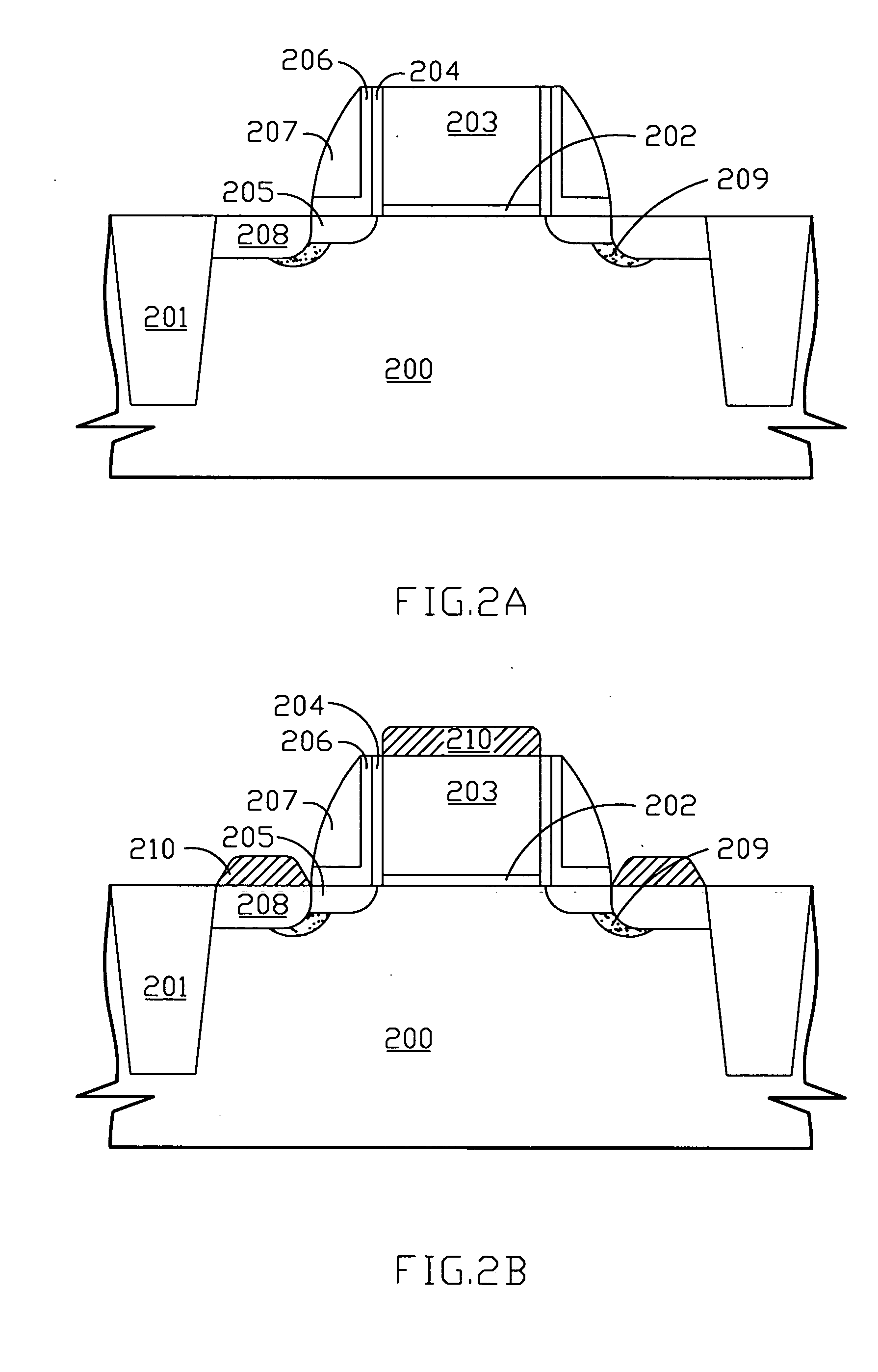
[0016] The present invention will be described in detail with reference to the accompanying drawings. The present invention provides a method of surface pretreatment before selective epitaxial growth process, which can resolve the undercut issue and surface roughness of the epitaxial layer. Referring to FIG.2A, a semiconductor substrate 200, such as a silicon substrate, with a first conductive type, is firstly provided. The first conductive type is either of N type and P type. A plurality of shallow trench isolations 201 is formed in the semiconductor substrate 200. Other isolation region, for example, field oxide, can be substituted for the shallow trench isolation 201. Then, a gate oxide 202 and a polysilicon gate electrode 203 are sequentially formed between each pair of the shallow trench isolations 201 on the semiconductor substrate 200. Next, forming an offset spacer of silicon dioxide 204 around the gate oxide 202 and the polysilicon gate electrode 203. Then, forming a lightl...


PUM


Abstract

A method of surface pretreatment before selective epitaxial growth is provided. A semiconductor substrate having metal-oxide-semiconductor devices formed thereon is provided, and a lightly dry etching process with a carbon-free plasma source is performed to remove a portion of the semiconductor substrate. Then, a selective epitaxial growth process is performed to form a semiconductor layer on the semiconductor substrate. A clean surface for selective epitaxial growth is provided by the lightly dry etching process, which can resolve the undercut issue and surface roughness.

Description

BACKGROUND OF THE INVENTION [0001] 1. Field of the Invention [0002] The present invention relates to a method of surface pretreatment in a semiconductor process, and more particularly to a method of surface pretreatment before selective epitaxial growth process. [0003] 2. Description of the Prior Art [0004] As semiconductor devices are scaled to smaller dimensions, generally in the sub-0.1 μm region, it is highly desirable and generally necessary to fabricate such devices with source / drain shallow junction. However, when a silicide is formed on the source / drain region, the silicide easily contacts with the shallow junction to make junction leakage. Therefore, an approach to resolve the leakage problem is to use raised source / drain. Since the raised source / drain is formed upward above the substrate, the silicide could not easily contact with the shallow junction, and then the junction leakage can be reduced. [0005]FIG. 1A to 1B shows various steps for forming a conventional N-channel...

Claims


Application Information

Patent Timeline
IPC IPC(8): C30B25/18H01L21/20H01L21/306H01L21/336
CPCC30B25/18H01L21/02046H01L21/02381H01L21/02532H01L29/66636H01L21/02639H01L29/665H01L29/6659H01L21/0262
Inventor CHIEN, CHIN-CHENGCHENG, YA-LUNWANG, YU-RENYANG, NENG-HUI
Owner UNITED MICROELECTRONICS CORP
Why Eureka
Try Eureka