Method for optimizing a number of kernels used in a sum of coherent sources for optical proximity correction in an optical microlithography process

a technology of optical proximity correction and kernel optimization, applied in the field of mask design, can solve the problems of increasing computation time and run time memory requirements, reducing the efficiency of coherent kernels, and reducing the efficiency of small elements of illumination sources

Inactive Publication Date: 2005-06-16
GLOBALFOUNDRIES INC
View PDF8 Cites 22 Cited by
  • Summary
  • Abstract
  • Description
  • Claims
  • Application Information

AI Technical Summary

Benefits of technology

[0009] Methods applied according to various exemplary embodiments of the present invention result in automatic optimization of the number of kernels N used in a SOCS simulation so that accuracy requirements are automatically satisfied and asymmetry is negligible.

Problems solved by technology

Increasing N improves SOCS accuracy, but also increases computation time and run time memory requirements.
Other choices (for example, forming a separate coherent kernel from each small element of the illumination source) are known to be less efficient.
This in turn may lead to different behavior of cells that are meant to be identical, which is highly undesirable.
However, such a manual approach is not reliable and can greatly increase turn-around time if the asymmetry is overlooked at the beginning of the process.
The problem is especially acute in situations that deal with an optical model having variable parameters or with a multiplicity of different optical models.

Method used


Image

  • Method for optimizing a number of kernels used in a sum of coherent sources for optical proximity correction in an optical microlithography process
  • Method for optimizing a number of kernels used in a sum of coherent sources for optical proximity correction in an optical microlithography process
  • Method for optimizing a number of kernels used in a sum of coherent sources for optical proximity correction in an optical microlithography process

Examples


Embodiment Construction

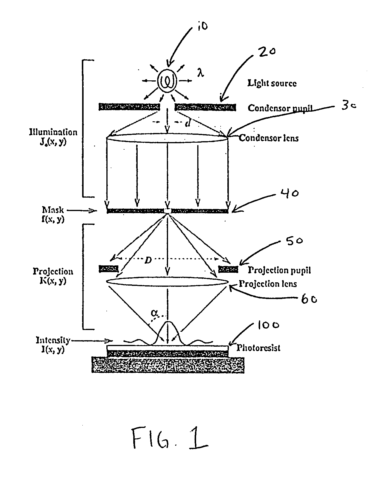
[0015] Current optical projection systems employed in optical lithography exclusively use partially coherent illumination. FIG. 1 is a schematic of a typical projection system. The projection system 1 includes a light source 10, a first condenser pupil 20, a first condenser lens 30, a mask 40, a second projection pupil 50, and a second projection lens 60. The projection system 1 in this case is used to form a pattern in a photoresist 100.

[0016] The process of partially coherent optical imaging may be described by the following nonlinear integral equation (the Hopkins model): I⁡(x,y)=⁢[T⁡(f)]⁢(x,y)=⁢∫∫∫∫f⁡(ξ1,ξ2)⁢J0⁡(ξ1,ξ2,η1,η2)⁢f*⁡(η1,η2)·⁢K⁡(x,y,ξ1,ξ2)⁢K*⁡(x,y,η1,η2)⁢ⅆξ1⁢ⅆξ2⁢ⅆη1⁢ⅆη2(1)

where: [0017] T( ) is the bilinear imaging operator; [0018] I( ) is the intensity image at the image plane; [0019] f( ) is the object being imaged (mask); [0020] K( ) is the coherent point spread function—describing properties of the projection system; and [0021] J0( ) is the mutual intensity func...


PUM

PropertyMeasurementUnit
light intensityaaaaaaaaaa
optical proximityaaaaaaaaaa
shapeaaaaaaaaaa

Abstract

A method for optimizing the number of kernels N used in a sum of coherent sources (SOCS) for optical proximity correction in an optical microlithography process including setting the number of kernels N to a predetermined minimum value Nmin. A determination is made as to whether an accuracy estimate of calculated intensity is within a tolerable value. A determination is also made as to whether an added X/Y asymmetry estimate of the calculated intensity is negligible.

Description

BACKGROUND OF THE INVENTION [0001] 1. Field of the Invention [0002] The present disclosure relates to optical microlithography, and more particularly to mask design. [0003] 2. Description of the Related Art [0004] Optical Proximity Correction (OPC) involves making systematic modifications to mask geometries in lithography to increase the achievable resolution and pattern transfer fidelity for IC manufacturing. This is accomplished by compensating mask geometry for known effects which will occur during imaging or subsequent processing. [0005] The essential part of a proximity correction apparatus is a simulation engine that provides an accurate simulation of the on-wafer shape, given an input shape on the mask. Conventional simulation engines use the Sum of Coherent Systems (SOCS) method, in which on-wafer light intensity for partially coherent illumination is decomposed into an incoherent sum of intensities from a nominally infinite number of coherent systems. For each particular “c...

Claims


Application Information

Patent Timeline
Patent Type & Authority Applications(United States)
IPC IPC(8): G03F1/14G06F17/10G06F17/50
CPCG03F1/36G03F1/144
Inventor GALLATIN, GREGG M.GOFMAN, EMANUELLAI, KAFAILAVIN, MARK A.MUKHERJEE, MAHARAJRAMM, DOVROSENBLUTH, ALAN EDWARDSHLAFMAN, SHLOMO
Owner GLOBALFOUNDRIES INC
Why Eureka
Try Eureka