Gap-fill method using high density plasma chemical vapor deposition process and method of manufacturing integrated circuit device

a chemical vapor deposition and high density plasma technology, applied in semiconductor/solid-state device manufacturing, basic electric elements, electric apparatus, etc., can solve the problem of increasing the process difficulty, and increasing the gap-filling characteristic. , to achieve the effect of preventing the formation of lung defects, and improving the gap-fill characteristi

Inactive Publication Date: 2005-06-23
SAMSUNG ELECTRONICS CO LTD
View PDF11 Cites 32 Cited by
  • Summary
  • Abstract
  • Description
  • Claims
  • Application Information

AI Technical Summary

Benefits of technology

[0014] Embodiments of the present invention provide a method of filling a gap by using an HDP-CVD process that has an improved gap-fill characteristic and prevents a lung defect from occurring.
[0015] Embodiments of the present invention also provide a method of manufacturing an integrated circuit device by using an HDP-CVD process that has an improved gap-fill characteristic and prevents a lung defect from occurring.
[0016] According to one feature of the present invention, there is provided a method of filling a gap by using an HDP-CVD process wherein, when an insulating layer created by the HDP-CVD process that fills a gap contains fluorine groups, the insulating layer is plasma treated with a process gas that includes hydrogen. Since the hydrogen in the process gas and the fluorine group react with each other by the plasma treatment to produce hydrogen fluoride, the fluorine groups can be removed from the insulating layer. Thus, a lung defect does not occur in the insulating layer and when a rinsing or wet etch process is carried out, a dent in the insulating layer is avoided.

Problems solved by technology

However, when the pattern is scaled down, an aspect ratio of gaps present between adjacent structures increases.
As a result, it is more difficult to completely fill the inside of a gap without causing a void.
However, as patterns have been further scaled down, this process has become inadequate.
When an argon gas has been used as a carrier gas in the HDP-CVD process to fill, for example, a gap of which width and aspect ratio are 0.15 μm and 4.5 or more, respectively, it has not been easy to completely fill the gap without causing a void.
The above limitation in the gap-fill characteristic of the HDP-CVD process is caused by the redeposition by sputtering.
If redeposition occurs excessively, the entrance of the gap may be closed by the redeposited material layer before completely filling the gap, which produces voids in the filled material layer.
However, both methods increase processing time and manufacturing cost.
As a result, it is difficult to apply them to mass production.
However, the method using chemical etch gas has a disadvantage in that a so-called lung defect can occur.
When a lung defect is created, an impurity gas remains in a gap-fill insulating layer, deteriorating the layer quality.

Method used


Image

  • Gap-fill method using high density plasma chemical vapor deposition process and method of manufacturing integrated circuit device
  • Gap-fill method using high density plasma chemical vapor deposition process and method of manufacturing integrated circuit device
  • Gap-fill method using high density plasma chemical vapor deposition process and method of manufacturing integrated circuit device

Examples


Embodiment Construction

[0024] Embodiments of the present invention will now be described more fully with reference to the accompanying drawings in which embodiments of the invention are shown. In the drawings, like reference numbers refer to like elements throughout and the sizes of elements may be exaggerated for clarity. Also, it will be understood that when an element such as a layer, region or substrate is referred to as being “on” or “onto” another element, it can be directly on the other element or intervening elements may also be present. Additionally, the layer, region or substrate could be partially within or partially embedded in another element.

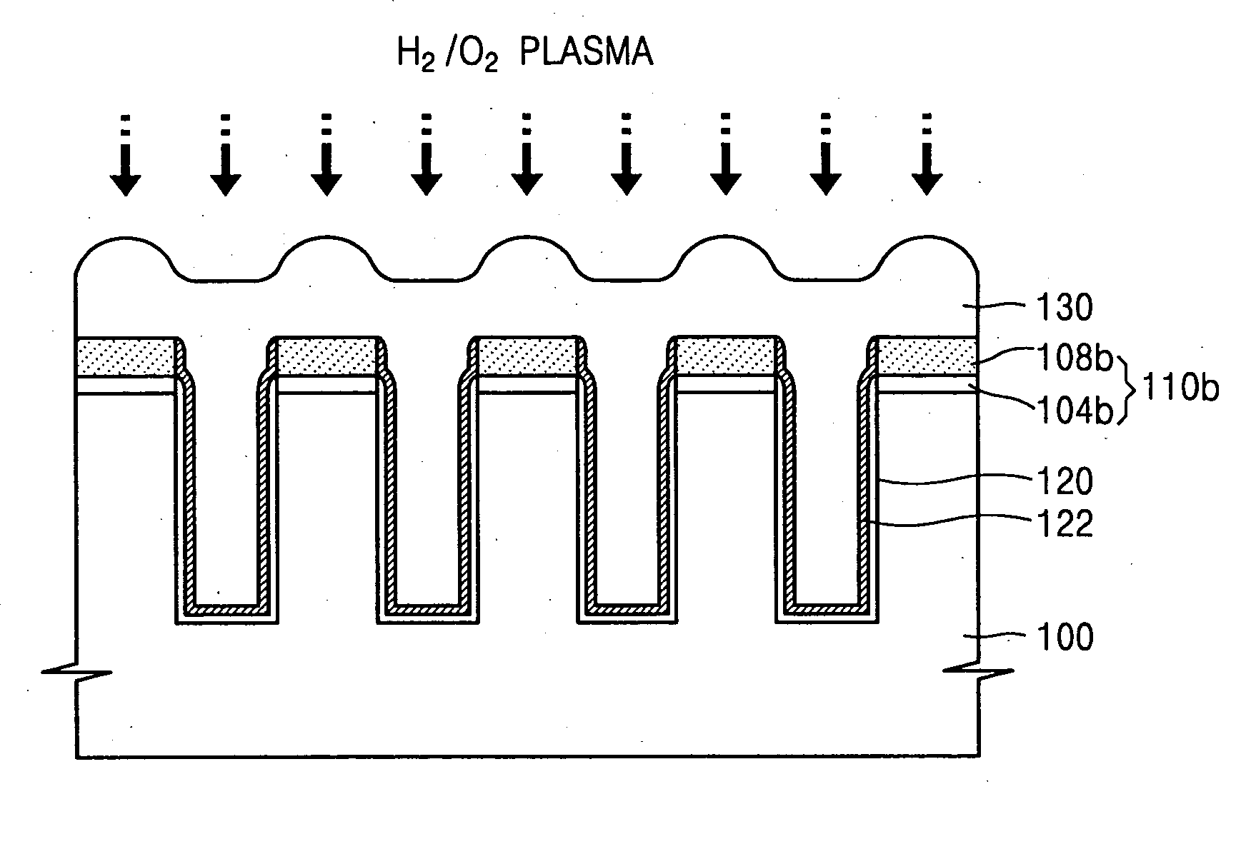
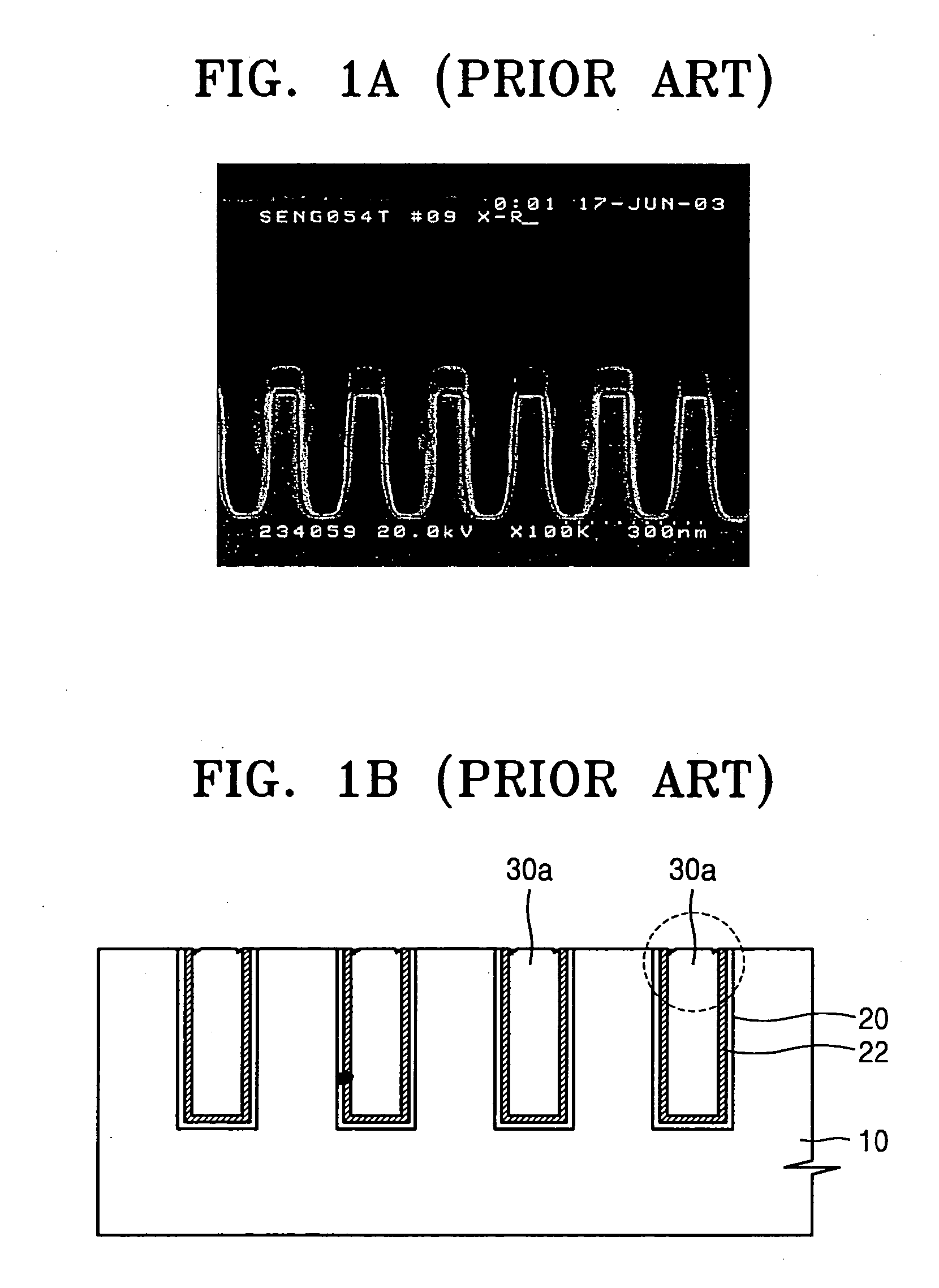
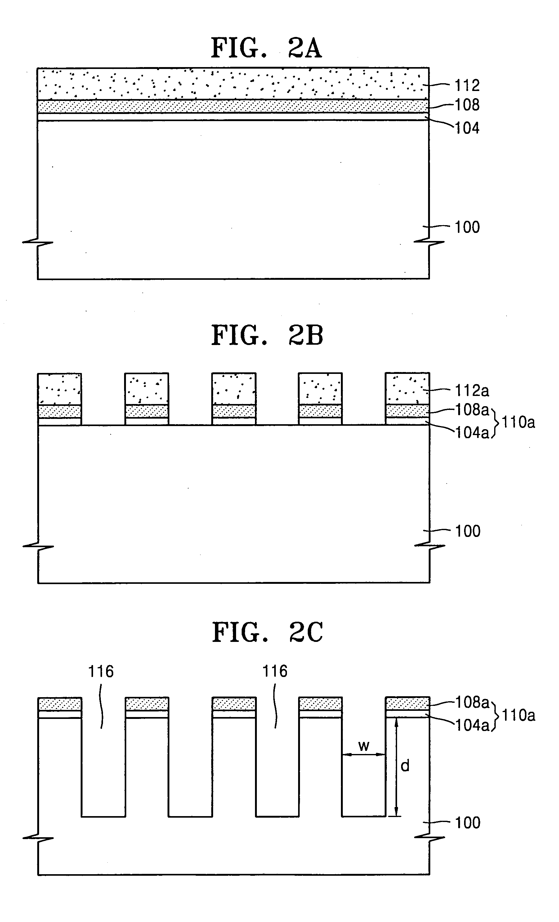
[0025] A gap-fill method according to an embodiment of the present invention includes plasma treating an integrated circuit substrate with hydrogen in addition to an HDP-CVD process using a process gas containing a fluorine group, thereby preventing a lung defect from occurring. The gap-fill method can be applied to a process for filling a gap with a hi...


PUM


Abstract

A method of filling gaps in an integrated circuit device is provided, that is less likely to fill voids and does not cause a lung defect. In one embodiment, a method of manufacturing an integrated circuit device including the gap filling method includes: etching a predetermined area of an integrated circuit device to form a trench, filling the trench with a high density plasma oxide by performing an HDP-CVD process using a first process gas including comprising a gas containing an element from the fluorine group, silane gas, and oxygen to form a high density plasma oxide layer, and plasma treating the integrated circuit substrate with a second process gas including a hydrogen gas or hydrogen and oxygen gases.

Description

[0001] This application claims priority from Korean Patent Application No. 2003-92562, filed on Dec. 17, 2003, the disclosure of which is incorporated herein by reference in its entirety. BACKGROUND OF THE INVENTION [0002] 1. Field of the Invention [0003] The present invention relates to a method of manufacturing an integrated circuit device, and more particularly, to a gap-fill method using a high density plasma chemical vapor deposition (HDP-CVD) process and a method of manufacturing an integrated circuit device. [0004] 2. Description of the Related Art [0005] Scaling down the pattern of an integrated circuit device is necessary for higher performance and higher integration. However, when the pattern is scaled down, an aspect ratio of gaps present between adjacent structures increases. As a result, it is more difficult to completely fill the inside of a gap without causing a void. Throughout the specification, the term “gap” refers to a recess present between two adjacent structur...

Claims


Application Information

Patent Timeline
Patent Type & Authority Applications(United States)
IPC IPC(8): H01L21/316H01L21/762H01L21/205H01L21/768
CPCH01L21/02164H01L21/02274H01L21/02304H01L21/0234H01L21/76837H01L21/76229H01L21/76802H01L21/76826H01L21/76831H01L21/31612H01L21/205
Inventor KIM, DO-HYUNGLEE, HYEON-DEOKLEE, JU-BUM
Owner SAMSUNG ELECTRONICS CO LTD
Why Eureka
Try Eureka