Organic electroluminescent device and method of fabricating the same
- Summary
- Abstract
- Description
- Claims
- Application Information
AI Technical Summary
Benefits of technology
Problems solved by technology
Method used
Image

Examples
first embodiment
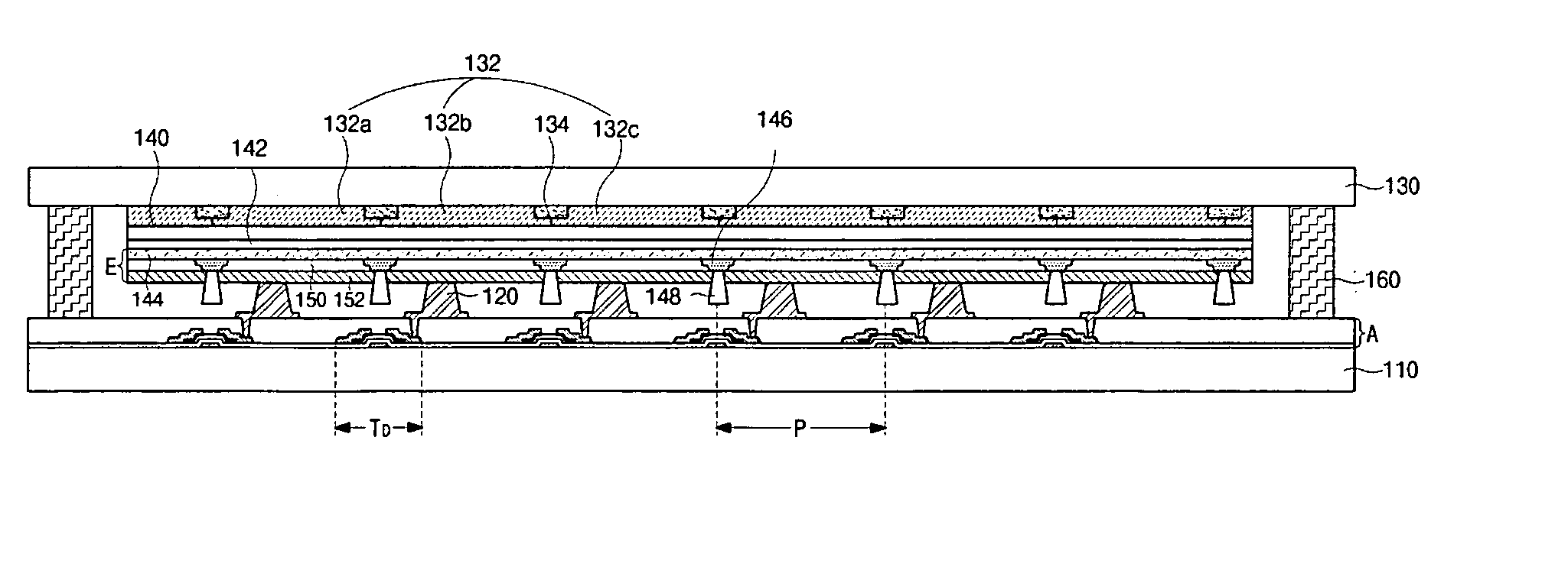
[0042]FIG. 3 is a cross-sectional view showing an organic electroluminescent device according to the present invention. As shown in FIG. 3, first and second substrates 110 and 130 face each other and are spaced apart from each other. An array layer “A” is formed on an inner surface of the first substrate 110. The array layer “A” includes a driving thin film transistor (TFT) “TD.” In contrast to the related art driving TFT “TD” shown in FIG. 2B having a top gate structure using polycrystalline silicon, the driving TFT “TD” shown in FIG. 3 has a bottom gate structure. Even though the driving TFT “TD” shown in FIG. 3 has a bottom gate structure using amorphous silicon, the driving TFT “TD” can alternatively have a top gate structure using polycrystalline silicon.
[0043] A black matrix 134 is formed on an inner surface of the second substrate 130 and a color filter layer 132 is formed on the black matrix 134. The color filter layer 132 includes red, green and blue sub-color filters 132a,...
second embodiment
[0048]FIG. 4 is a cross-sectional view showing an organic electroluminescent device according to the present invention. As shown in FIG. 4, first and second substrates 210 and 230 face each other and are spaced apart from each other. An array layer “A,” including a driving thin film transistor (TFT) “TD” having a bottom gate structure, is formed on an inner surface of the first substrate 110. Even though the driving TFT “TD” shown in FIG. 4 has a bottom gate structure using amorphous silicon, the driving TFT “TD” can alternatively have a top gate structure using polycrystalline silicon.
[0049] A first electrode 244 is formed on an inner surface of the second substrate 230. An interlayer insulating layer 246 and a separator 248 having a taper shape are sequentially formed on the first electrode 244 at a boundary portion of a pixel region “P.” An organic luminescent layer 250 including red, green and blue sub-luminescent layers 250a, 250b and 250c and a second electrode 252 are sequent...
third embodiment
[0052]FIG. 5 is a cross-sectional view showing an organic electroluminescent device according to the present invention. As shown in FIG. 5, first and second substrates 310 and 330 face each other and are spaced apart from each other. An array layer “A,” including a driving thin film transistor (TFT) “TD,” is formed on an inner surface of the first substrate 310. Even though the driving TFT “TD” shown in FIG. 5 has a bottom gate structure using amorphous silicon, the driving TFT “TD” can alternatively have a top gate structure using polycrystalline silicon.
[0053] A black matrix 334 is formed on an inner surface of the second substrate 330 and a color filter layer 332 is formed on the black matrix 334. The color filter layer 332 includes red, green and blue sub-color filters 332a, 332b and 332c and the black matrix 334 surrounds each sub-color filter. A planarization layer 340 of an insulating material is formed on the color filter layer 332. For example, the planarization layer 340 i...
PUM
 Abstract
Description
Claims
Application Information
 - Generate Ideas
- Intellectual Property
- Life Sciences
- Materials
- Tech Scout
- Unparalleled Data Quality
- Higher Quality Content
- 60% Fewer Hallucinations
Browse by: Latest US Patents, China's latest patents, Technical Efficacy Thesaurus, Application Domain, Technology Topic, Popular Technical Reports.
© 2025 PatSnap. All rights reserved.Legal|Privacy policy|Modern Slavery Act Transparency Statement|Sitemap|About US| Contact US: help@patsnap.com